Surface Mount Technology (SMT) soldering is a critical process in modern electronics manufacturing. The quality of SMT soldering directly impacts the reliability, performance, and longevity of electronic devices. As technology advances and components become smaller and more complex, maintaining high soldering quality becomes increasingly challenging. This comprehensive guide explores the various elements that influence SMT soldering quality and presents effective improvement measures to enhance the overall soldering process.

Understanding SMT Soldering
What is SMT Soldering?
Surface Mount Technology (SMT) soldering is a method used to mount electronic components directly onto the surface of printed circuit boards (PCBs). This technique has largely replaced through-hole technology in many applications due to its ability to achieve higher component density, improved performance, and reduced production costs.
Key Advantages of SMT Soldering
| Advantage | Description |
| Miniaturization | Allows for smaller, more compact electronic devices |
| Increased component density | More components can be placed on a single PCB |
| Improved performance | Shorter electrical paths lead to better high-frequency performance |
| Automated assembly | Highly suitable for automated production processes |
| Cost-effectiveness | Reduced material costs and increased production efficiency |
Elements Influencing SMT Soldering Quality

1. PCB Design and Quality
PCB Material Selection
The choice of PCB material significantly impacts soldering quality:
PCB Surface Finish
Different surface finishes affect solderability:
- HASL (Hot Air Solder Leveling)
- ENIG (Electroless Nickel Immersion Gold)
- OSP (Organic Solderability Preservative)
- Immersion Tin
- Immersion Silver
Pad Design
Proper pad design is crucial for successful soldering:
- Pad size and shape
- Solder mask clearance
- Via-in-pad design considerations
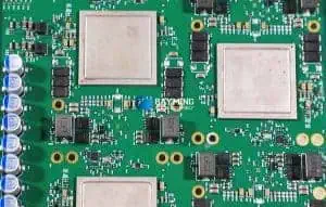
2. Component Factors
Component Package Types
Various package types present different soldering challenges:
- Quad Flat Packages (QFP)
- Ball Grid Arrays (BGA)
- Chip Scale Packages (CSP)
- Leadless packages (e.g., QFN, LGA)
Component Quality and Storage
- Moisture sensitivity levels (MSL)
- Proper storage and handling
- Component age and oxidation
Component Placement Accuracy
- Pick and place machine calibration
- Component alignment
- Placement force
3. Solder Paste Characteristics
Solder Alloy Composition
Common solder alloys and their properties:
| Alloy | Composition | Melting Point | Applications |
| SAC305 | Sn96.5/Ag3.0/Cu0.5 | 217-220°C | General purpose lead-free |
| SN100C | Sn/Cu0.7/Ni0.05/Ge0.005 | 227°C | Lead-free, good fatigue resistance |
| SnPb | Sn63/Pb37 | 183°C | Legacy leaded solder (restricted use) |
Solder Paste Particle Size
- Type 3 (25-45 μm)
- Type 4 (20-38 μm)
- Type 5 (15-25 μm)
Solder Paste Rheology
- Viscosity
- Thixotropic properties
- Slump resistance
4. Stencil Design and Quality
Stencil Thickness
- Standard thickness (4-6 mil)
- Step stencils for mixed component types
Aperture Design
- Area ratio considerations
- Aspect ratio optimization
- Custom aperture shapes for specific components
Stencil Material and Manufacturing
- Stainless steel vs. nickel stencils
- Laser-cut vs. electroformed stencils
- Nano-coated stencils for improved release
5. Printing Process Parameters
Printing Speed and Pressure
- Optimal print speed for different paste types
- Squeegee pressure adjustment
Squeegee Type and Angle
- Metal vs. polyurethane squeegees
- Squeegee angle impact on paste deposit
Snap-off Distance
- Zero vs. positive snap-off
- Impact on paste transfer efficiency
6. Reflow Profile Optimization
Reflow Zones and Their Functions

| Zone | Function | Temperature Range |
| Preheat | Activate flux, gradually heat PCB | 150-180°C |
| Soak | Equalize temperatures across the board | 180-210°C |
| Reflow | Melt solder, form joints | Above liquidus (e.g., 220-250°C for SAC305) |
| Cooling | Solidify solder joints | Ramp down to room temperature |
Critical Profile Parameters
- Ramp rate (°C/second)
- Time above liquidus
- Peak temperature
- Cooling rate
Profile Considerations for Different Components
- Large thermal mass components
- Temperature-sensitive components
- Mixed component types on a single PCB
7. Reflow Oven Capabilities
Heating Technologies
- Convection (forced air)
- Infrared (IR)
- Vapor phase
Temperature Control and Uniformity
- Number of heating zones
- Temperature sensors and feedback systems
- Conveyor speed control
Atmosphere Control
- Nitrogen vs. air atmosphere
- Oxygen level monitoring
8. Post-Reflow Processes
Cooling Rate Control
- Natural vs. forced cooling
- Impact on solder joint microstructure
Cleaning Processes (if applicable)
- No-clean vs. clean processes
- Cleaning agent selection
- Cleaning equipment considerations
Inspection and Quality Control
Improvement Measures for SMT Soldering Quality
1. Design for Manufacturability (DFM)
PCB Layout Optimization
- Component placement guidelines
- Thermal relief for large pads
- Balanced thermal design
Standardization of Pad Designs
- Create a library of optimized pad designs
- Ensure consistency across different projects
Collaborative Design Reviews
- Involve manufacturing engineers in the design process
- Regular design review meetings with all stakeholders
2. Component Management
Implement Moisture Sensitive Device (MSD) Controls
- Proper storage in dry cabinets
- Tracking of floor life
- Baking procedures when necessary
Incoming Quality Control
- Sample testing of incoming components
- X-ray inspection for BGAs and other hidden-joint packages
First Article Inspection
- Detailed inspection of first production run
- Verification of component placement and orientation
3. Solder Paste Optimization
Regular Solder Paste Testing
| Test | Purpose | Frequency |
| Viscosity | Ensure consistent printing | Daily |
| Solder ball test | Check reflow performance | Weekly |
| Print quality inspection | Verify stencil release and definition | Every shift |
| Wetting balance test | Assess solderability | Monthly |
Proper Solder Paste Handling
- Temperature-controlled storage
- Adherence to manufacturer’s recommendations for kneading and usage
Continuous Improvement in Paste Selection
- Evaluate new solder paste formulations
- Conduct trials with different particle sizes for fine-pitch applications
4. Stencil Design and Maintenance
Optimize Aperture Design
- Use area ratio and aspect ratio calculations
- Implement custom apertures for challenging components
Regular Stencil Cleaning and Inspection

- Implement automated under-stencil cleaning systems
- Periodically inspect for wear or damage
Explore Advanced Stencil Technologies
- Evaluate nano-coated stencils for improved release
- Consider step stencils for mixed-technology boards
5. Print Process Optimization
Statistical Process Control (SPC) for Printing
- Implement automated solder paste inspection (SPI)
- Track key metrics like volume, area, and height of paste deposits
Regular Printer Maintenance and Calibration
- Develop a preventive maintenance schedule
- Calibrate critical parameters (e.g., alignment, pressure) regularly
Optimize Printing Parameters
- Conduct design of experiments (DOE) to find optimal settings
- Regularly review and update printing parameters
6. Reflow Profile Optimization
Utilize Profiling Software and Equipment
- Invest in advanced profiling tools
- Create a library of optimized profiles for different board types
Implement Adaptive Profiling
- Use real-time monitoring systems
- Adjust profiles based on actual board temperatures
Conduct Regular Thermal Profiling
- Profile new board designs
- Periodically re-profile existing products to account for oven drift
7. Reflow Oven Maintenance and Upgrade
Regular Oven Maintenance
- Clean and calibrate on a scheduled basis
- Replace worn components (e.g., conveyor belts, heating elements)
Implement Closed-loop Temperature Control
- Use multiple thermocouples for accurate temperature mapping
- Integrate feedback systems for real-time adjustments
Consider Advanced Reflow Technologies
- Evaluate vapor phase soldering for challenging applications
- Explore selective soldering for mixed-technology boards
8. Post-Reflow Process Improvements
Optimize Cooling Strategies
- Implement controlled cooling zones
- Consider nitrogen cooling for sensitive components
Enhance Inspection Processes
- Integrate multiple inspection technologies (AOI, AXI, ICT)
- Develop comprehensive inspection criteria
Implement Effective Failure Analysis
- Establish a dedicated failure analysis lab
- Use root cause analysis techniques to address recurring issues
Conclusion
Achieving and maintaining high-quality SMT soldering requires a comprehensive approach that addresses all aspects of the manufacturing process. By understanding the various elements that influence soldering quality and implementing targeted improvement measures, manufacturers can significantly enhance their SMT soldering processes. This, in turn, leads to improved product reliability, reduced defects, and increased customer satisfaction.
Continuous improvement should be at the core of any SMT soldering quality initiative. Regular evaluation of new technologies, materials, and techniques, coupled with ongoing training and development of personnel, will ensure that your SMT soldering processes remain at the cutting edge of industry standards.
Remember that soldering quality is not just about the end result but also about consistency and repeatability. By implementing robust processes, leveraging data-driven decision-making, and fostering a culture of quality throughout the organization, manufacturers can achieve excellence in SMT soldering and maintain a competitive edge in the ever-evolving electronics industry.
Frequently Asked Questions (FAQ)
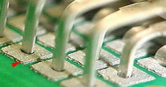
Q1: What are the most common SMT soldering defects, and how can they be prevented?
A1: Common SMT soldering defects include:
- Solder bridges: Excess solder connecting adjacent pads or leads. Prevention: Optimize stencil design, control solder paste volume, and ensure proper component placement.
- Insufficient solder: Not enough solder to form a proper joint. Prevention: Adjust stencil aperture design, ensure proper solder paste printing, and optimize reflow profile.
- Tombstoning: One end of a component lifts off the pad during reflow. Prevention: Balance pad designs, ensure even heating during reflow, and consider component placement orientation.
- Voiding: Voids or air pockets within the solder joint. Prevention: Use low-voiding solder pastes, optimize reflow profile, and consider vacuum reflow for critical applications.
- Head-in-pillow: Incomplete wetting between BGA ball and pad. Prevention: Optimize reflow profile, use flux-rich solder pastes, and ensure proper handling of moisture-sensitive devices.
Preventing these defects requires a holistic approach, addressing PCB design, component quality, process parameters, and equipment maintenance.
Q2: How does the transition to lead-free soldering affect SMT quality, and what adjustments are necessary?
A2: The transition to lead-free soldering has several impacts on SMT quality:
- Higher melting point: Lead-free alloys typically melt at higher temperatures, requiring adjustments to reflow profiles.
- Wetting behavior: Lead-free solders generally have poorer wetting characteristics, which can affect joint formation.
- Increased voiding: Some lead-free alloys are more prone to voiding, especially in BGA joints.
- Different microstructure: Lead-free joints have a different microstructure, which can affect long-term reliability.
Necessary adjustments include:
- Updating reflow profiles to accommodate higher temperatures
- Optimizing pad and stencil designs for lead-free pastes
- Using more active fluxes to improve wetting
- Implementing nitrogen reflow to enhance wetting and reduce oxidation
- Increasing focus on thermal management due to higher process temperatures
- Enhancing cleaning processes if using higher activity fluxes
- Updating inspection criteria to account for the different appearance of lead-free joints
Q3: What role does nitrogen atmosphere play in SMT soldering, and when is it beneficial to use?
A3: Nitrogen atmosphere in SMT soldering can provide several benefits:
- Improved wetting: Reduces surface tension of molten solder, enhancing wetting.
- Reduced oxidation: Prevents oxidation of pad surfaces and solder paste during reflow.
- Better thermal transfer: Nitrogen has better heat transfer properties than air.
- Improved joint appearance: Often results in shinier, smoother solder joints.
- Potential for reduced defects: Can help reduce issues like voiding and non-wetting.
Nitrogen is particularly beneficial in the following situations:
- When using lead-free solders, which generally have poorer wetting characteristics
- For fine-pitch or challenging components like BGAs and QFNs
- In high-reliability applications where joint quality is critical
- When processing boards with poor solderability or long shelf life
- For products that require optimal cosmetic appearance of solder joints
However, nitrogen systems add cost and complexity to the reflow process. The decision to use nitrogen should be based on a cost-benefit analysis, considering factors like product requirements, defect rates, and production volume.
Q4: How can manufacturers effectively manage the soldering of boards with mixed component types and thermal masses?
A4: Managing boards with mixed component types and thermal masses requires a multi-faceted approach:
- PCB Design:
- Group components with similar thermal characteristics
- Use thermal relief pads for large components
- Consider split planes to manage heat distribution
- Stencil Design:
- Implement step stencils to vary paste volume for different component types
- Use custom apertures for unique component requirements
- Reflow Profile Optimization:
- Develop a profile that balances the needs of all components
- Use longer soak times to equalize temperatures across the board
- Consider ramp-to-spike profiles for boards with extreme mix
- Oven Configuration:
- Use ovens with more heating zones for better profile control
- Implement bottom-side heating for large thermal mass components
- Component Placement:
- Place large thermal mass components on the same side of the board
- Avoid placing temperature-sensitive components near high thermal mass ones
- Use of Selective Soldering:
- Consider selective soldering for through-hole components on mixed-technology boards
- Thermal Profiling:
- Use multiple thermocouples to monitor different areas of the board
- Perform comprehensive profiling for each new board design
- Simulation and Modeling:
- Use thermal simulation software to predict heat distribution
- Optimize designs based on simulation results
By combining these strategies, manufacturers can achieve consistent soldering quality across all components, regardless of their thermal characteristics.
Q5: What are the key considerations for implementing a robust SMT soldering quality control process?
A5: Implementing a robust SMT soldering quality control process involves several key considerations:
- In-Process Monitoring:
- Implement automated solder paste inspection (SPI) after printing
- Use in-line AOI (Automated Optical Inspection) after placement and post-reflow
- Consider real-time process parameter monitoring (e.g., oven temperatures, conveyor speed)
- End-of-Line Inspection:
- Implement final AOI for comprehensive defect detection
- Use X-ray inspection for hidden joints (e.g., BGAs, bottom-terminated components)
- Perform In-Circuit Testing (ICT) or Flying Probe Testing for electrical verification
- Statistical Process Control (SPC):
- Track key metrics like defect rates, first-pass yield, and process capability indices
- Implement control charts to monitor process stability
- Use trend analysis to identify potential issues before they become critical
- Failure Analysis:
- Establish a dedicated failure analysis lab
- Implement root cause analysis procedures for defects
- Use tools like cross-sectioning and scanning electron microscopy for detailed analysis