Introduction
Insulated Gate Bipolar Transistors (IGBTs) have become indispensable components in modern industrial applications, ranging from sophisticated motor drive systems to advanced electrical control circuits. These semiconductor devices are particularly valued for their ability to achieve significantly lower switching losses compared to conventional alternatives, making them essential for energy-efficient power electronics. However, the operational reliability of IGBTs extends beyond their switching performance to include their ability to withstand fault conditions, particularly short-circuit events.
During normal operation, IGBTs must demonstrate robust short-circuit withstand capability to ensure system reliability and safety. However, when short-circuit oscillations (SCOs) occur during fault conditions, the IGBT’s ability to survive these events can be severely compromised. These oscillations not only threaten the device’s structural integrity but can also generate electromagnetic interference (EMI) hazards when the oscillation amplitude becomes excessive and the collector-emitter voltage (VCE) range spans too broadly. Consequently, understanding and optimizing SCO behavior under short-circuit conditions has become a critical aspect of IGBT design and application.
Fundamental Mechanisms of Short-Circuit Oscillations
The root cause of short-circuit oscillations in IGBTs lies in the complex interplay between charge carrier dynamics and electric field distributions within the device structure. Unlike conventional design parameters that affect basic IGBT characteristics, SCO behavior is primarily influenced by the backside design elements, specifically the Field Stop (FS) layer and P+ emitter configurations. These structural components directly impact the bipolar current gain coefficient (αpnp) of the IGBT’s inherent pnp transistor, which plays a pivotal role in determining oscillation characteristics.
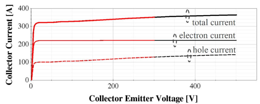
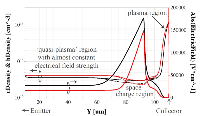
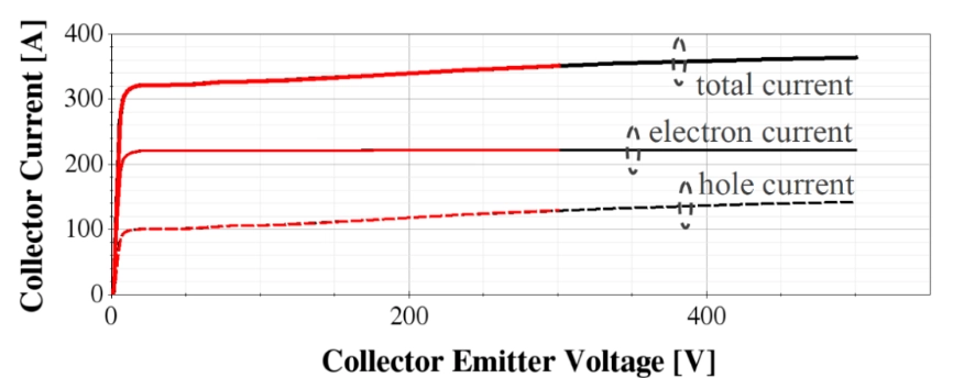
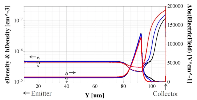
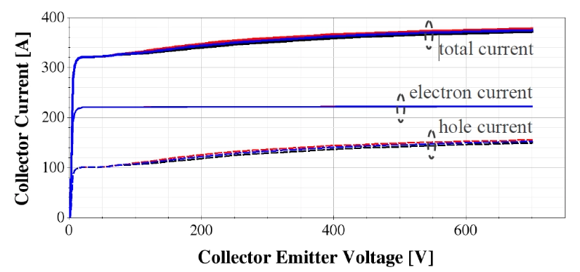
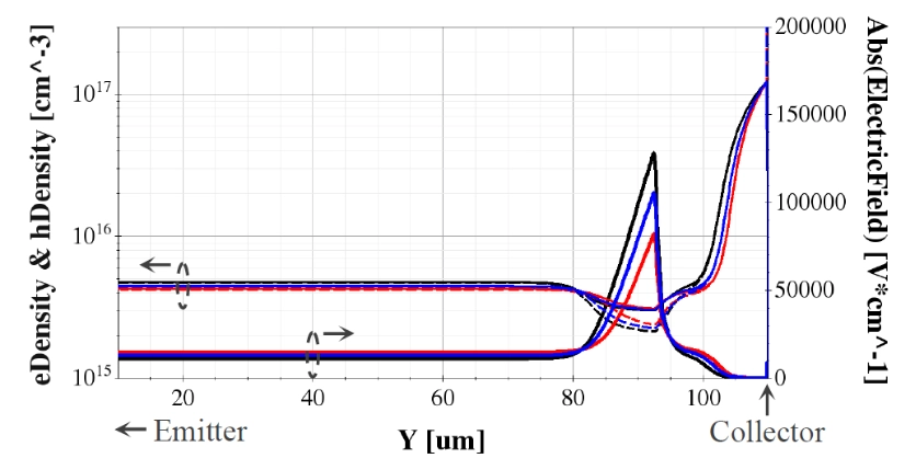
To understand this phenomenon, consider the IGBT structure under steady-state conditions at a constant junction temperature. When examining the output characteristics at different collector-emitter voltages (300V and 500V), distinct regions emerge within the device: the quasi-plasma region, the space charge region, and the plasma region. The vertical distribution of electric field intensity and carrier density reveals that high electric field intensity in the FS region results from negative space charges accumulated in the drift region.
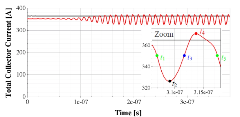
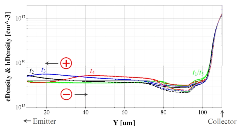
The oscillation mechanism becomes apparent when analyzing transient behavior during short-circuit conditions. The periodic storage and release of charge carriers within the device, combined with corresponding variations in electric field distribution, creates the characteristic high-frequency oscillations observed in short-circuit conditions. This phenomenon manifests as electrons and holes being alternately stored within the device structure and then released in surge-like formations that propagate through different regions of the IGBT.
During the initial phase of oscillation, charge carriers accumulate primarily in the internal regions of the device. As the oscillation progresses, a charge-carrier plasma surge gradually forms and begins propagating through the device structure. This surge eventually reaches the FS region, where it triggers the release of stored electrons and holes. The cyclical nature of this storage and release process, coupled with the dynamic electric field redistribution, sustains the oscillation behavior and determines its frequency characteristics.
Impact of Device Structure on Oscillation Behavior
P+ Emitter Dose Effects
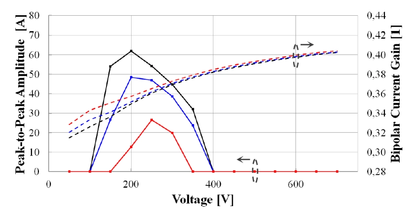
The concentration of dopants in the P+ emitter region significantly influences the IGBT’s short-circuit oscillation characteristics. Experimental analysis reveals that the emitter dose effect on hole injection and the bipolar current gain coefficient (αpnp) is most pronounced at collector-emitter voltages below 250V. This voltage range corresponds to the region where SCOs typically initiate and are most problematic.
When the P+ emitter dose is increased, several important changes occur in the device’s internal structure and behavior. The remaining plasma region located in front of the P+ emitter expands, and its maximum carrier density level increases correspondingly. This enhancement in plasma characteristics leads to a slight increase in electric field intensity within the drift region preceding the FS layer, while simultaneously causing a slight reduction in field intensity within the FS layer itself.
The relationship between P+ emitter dose and oscillation behavior follows a predictable pattern: as the emitter dose increases, the bipolar current gain coefficient (αpnp) also increases. This increase in αpnp correlates directly with a reduction in both the voltage range over which SCOs occur and the amplitude of the oscillations themselves. This relationship suggests that optimizing the P+ emitter dose can be an effective strategy for mitigating problematic oscillation behavior.
FS Layer Dose Optimization
The Field Stop layer dose represents another critical parameter in controlling short-circuit oscillations. For collector-emitter voltages exceeding 50V, the FS layer dose demonstrates significant influence over hole injection characteristics and the resulting αpnp values. This influence extends across a broader voltage range compared to the P+ emitter dose effects, making FS layer optimization particularly important for comprehensive oscillation control.
Reducing the FS layer dose produces notable changes in the device’s internal carrier distribution. The plasma region positioned in front of the P+ emitter contracts, leading to alterations in the overall charge carrier dynamics. These changes manifest as modifications in both the voltage range where SCOs occur and their amplitude characteristics.
Interestingly, as the FS layer dose decreases and αpnp increases, the voltage range where SCOs occur shifts toward lower voltages. However, this shift is accompanied by beneficial reductions in both the overall voltage range affected by oscillations and the amplitude of the oscillations themselves. This behavior indicates that FS layer dose optimization can provide a pathway for minimizing oscillation-related problems while potentially shifting their occurrence to less critical operating conditions.
Temperature Dependencies and Thermal Effects
Junction temperature plays a multifaceted role in determining short-circuit oscillation behavior, affecting both hole current and channel current characteristics simultaneously. Temperature variations create complex changes in the device’s internal physics, influencing carrier mobility, injection efficiency, and field distribution patterns.
As junction temperature increases, the plasma region in front of the P+ emitter undergoes contraction, leading to modified charge carrier dynamics throughout the device structure. This thermal effect on plasma distribution directly impacts the oscillation characteristics, generally leading to reductions in both the voltage range affected by SCOs and their amplitude.
The temperature dependence of αpnp reveals additional complexity in the thermal behavior of SCOs. At lower collector-emitter voltages, αpnp decreases as junction temperature rises, likely due to reduced carrier mobility at elevated temperatures. This temperature-mobility relationship creates a natural suppression mechanism for oscillations at higher operating temperatures, suggesting that thermal management strategies could be incorporated into oscillation mitigation approaches.
Optimization Strategies and Design Trade-offs
Backside Design Approaches
Effective mitigation of short-circuit oscillations requires careful attention to backside design parameters, particularly those affecting the bipolar current gain coefficient under short-circuit conditions. The primary strategy involves increasing αpnp to levels sufficient for oscillation suppression or elimination. When αpnp reaches appropriately high values, SCOs can be completely avoided, providing a definitive solution to oscillation-related problems.
However, this optimization approach introduces important design trade-offs that must be carefully considered. Increasing αpnp to suppress oscillations inevitably leads to higher leakage currents during normal operation, which can impact device efficiency and power consumption. Additionally, turn-off losses increase, potentially offsetting some of the switching advantages that make IGBTs attractive for many applications.
Thermal Stability Considerations
Perhaps most critically, enhancing αpnp to eliminate SCOs can compromise thermal short-circuit stability, creating a complex optimization challenge. Device designers must balance oscillation suppression against thermal performance, leakage characteristics, and switching losses to achieve optimal overall performance.
This multifaceted trade-off requires comprehensive analysis of the specific application requirements and operating conditions. For applications where SCO suppression is paramount, accepting increased leakage and switching losses may be justified. Conversely, for applications where thermal performance and efficiency are critical, alternative approaches to oscillation management may be necessary.
Advanced Analysis and Future Directions
The relationship between oscillation amplitude and voltage range provides insights into the underlying physics governing SCO behavior. The peak-to-peak collector current amplitude serves as a quantitative measure of oscillation intensity, enabling systematic comparison of different design approaches and parameter optimization strategies.
Detailed analysis of carrier density distributions at various time points during oscillation cycles reveals the dynamic nature of charge carrier movement and storage within the device. These distributions demonstrate how carrier surges propagate through different device regions and how the timing of these movements influences overall oscillation characteristics.
Conclusion
Short-circuit oscillations in IGBTs represent a complex phenomenon requiring careful analysis of multiple interdependent factors. The periodic storage and release of charge carriers, driven by dynamic electric field distributions, creates the fundamental mechanism underlying these oscillations. Through systematic optimization of backside design parameters, particularly P+ emitter dose and FS layer dose, significant improvements in SCO behavior can be achieved.
The key to successful oscillation mitigation lies in understanding the role of the bipolar current gain coefficient (αpnp) and implementing design strategies that increase this parameter to appropriate levels. However, the inevitable trade-offs between oscillation suppression and other device characteristics necessitate careful consideration of specific application requirements.
Temperature effects provide both challenges and opportunities for oscillation management, with higher junction temperatures naturally suppressing SCO behavior. This thermal dependence suggests that integrated approaches combining structural optimization with thermal management could provide comprehensive solutions to oscillation-related problems.
Future developments in IGBT design will likely focus on advanced modeling techniques that can predict SCO behavior more accurately and enable optimization strategies that minimize the trade-offs inherent in current approaches. Understanding these complex interactions remains essential for continued advancement in power semiconductor technology and the development of more robust, efficient IGBT devices for demanding industrial applications.