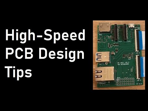
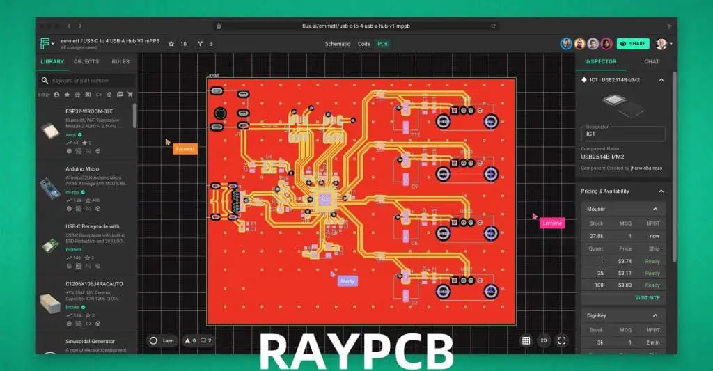
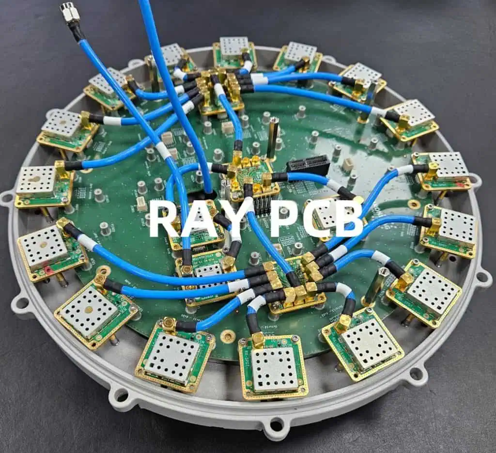
As digital systems continue to push the boundaries of speed and performance, high-speed PCB design has become increasingly complex. Channel Operating Margin (COM) has emerged as a critical metric for ensuring signal integrity and reliable data transmission in high-speed digital designs. This comprehensive guide explores COM analysis, its implementation, and best practices for optimizing high-speed PCB designs.

Understanding Channel Operating Margin
Definition and Fundamentals
Channel Operating Margin represents a unified figure of merit that quantifies the performance and reliability of high-speed serial links. It combines various channel impairments and characteristics into a single numerical value, making it easier for designers to assess link viability. COM is typically expressed in decibels (dB), with higher values indicating better channel performance.
Key Components of COM Analysis
Signal Impairments
- Inter-Symbol Interference (ISI)
- Crosstalk (NEXT and FEXT)
- Random and deterministic jitter
- Channel noise
- Reflection effects
Design Parameters
- Transmission line characteristics
- PCB material properties
- Via transitions
- Connector specifications
- Terminal impedance matching
COM Calculation Methodology

Mathematical Framework
COM calculations involve complex mathematical models that consider both frequency-domain and time-domain analyses. The basic COM equation can be expressed as:
COM (dB) = 20 * log10(Signal Amplitude / Noise + Interference)Standard Requirements
| Specification | Minimum COM Requirement (dB) | Target Operating Speed |
| PCIe Gen 4.0 | 3 | 16 GT/s |
| PCIe Gen 5.0 | 4 | 32 GT/s |
| 112G PAM4 | 5 | 112 Gbps |
| 400GbE | 3 | 53.125 GBd |
Design Optimization Strategies
Transmission Line Optimization
Impedance Control
Maintaining consistent impedance throughout the channel is crucial for optimal COM performance. Consider the following target impedances for different applications:
| Application Type | Single-Ended Impedance (Ω) | Differential Impedance (Ω) |
| PCIe | 50 ±10% | 100 ±10% |
| DDR4 | 40 ±10% | 80 ±10% |
| USB 3.x | 45 ±10% | 90 ±10% |
Material Selection Guidelines
Dielectric Materials
| Material Type | Dk Range | Df Range | Recommended Applications |
| FR-4 | 4.0-4.5 | 0.02-0.03 | Up to 10 Gbps |
| Megtron 6 | 3.4-3.6 | 0.002-0.004 | Up to 56 Gbps |
| PTFE | 2.1-2.5 | 0.001-0.002 | Above 56 Gbps |
Layout Optimization Techniques
Trace Routing Guidelines
- Maintain minimum spacing between differential pairs
- Avoid sharp corners and use curved or 45-degree traces
- Minimize via count and optimize via placement
- Implement proper reference plane design
Via Design Optimization
Via Parameters for Different Speed Grades
| Speed Grade | Via Diameter (mils) | Anti-Pad Diameter (mils) | Backdrilling Depth |
| < 10 Gbps | 10.-12 | 20-24 | Optional |
| 10-28 Gbps | 8.-10 | 18-20 | Recommended |
| > 28 Gbps | 6.-8 | 16-18 | Required |
Advanced COM Analysis Techniques

Pre-Layout Analysis
Before beginning the physical design, perform these essential analyses:
- Channel budget allocation
- Material selection verification
- Preliminary stackup design
- Initial COM predictions
Post-Layout Verification
COM Measurement Points
| Measurement Location | Purpose | Typical COM Threshold |
| Transmitter Output | Initial signal quality | > 6 dB |
| After First Connector | Connector impact | > 5 dB |
| Receiver Input | Final signal quality | > 3 dB |
Implementation Case Studies
Case Study 1: PCIe Gen 5 Design
Design Parameters
- Operating speed: 32 GT/s
- Channel length: 12 inches
- Layer count: 16
- Material: Modified Megtron 6
Results
| Parameter | Target | Achieved | Margin |
| COM | 4.0 dB | 4.8 dB | +0.8 dB |
| Return Loss | -12 dB | -14 dB | +2.0 dB |
| Insertion Loss | -20 dB | -18 dB | +2.0 dB |
Case Study 2: 112G PAM4 Design
Design Parameters
- Operating speed: 112 Gbps
- Channel length: 8 inches
- Layer count: 24
- Material: Low-loss PTFE
Results
| Parameter | Target | Achieved | Margin |
| COM | 5.0 dB | 5.3 dB | +0.3 dB |
| Return Loss | -15 dB | -16 dB | +1.0 dB |
| Insertion Loss | -22 dB | -21 dB | +1.0 dB |
Best Practices and Recommendations
Design Checklist
- Pre-layout Phase
- Material selection verification
- Stackup optimization
- Initial COM analysis
- Layout Phase
- Impedance-controlled routing
- Via optimization
- Reference plane design
- Post-layout Phase
- COM verification
- Design rule checking
- Manufacturing feasibility review
Frequently Asked Questions
1. What is the minimum acceptable COM value for high-speed designs?
The minimum acceptable COM value varies by application and standard. Generally:
- PCIe Gen 4.0: ≥ 3.0 dB
- PCIe Gen 5.0: ≥ 4.0 dB
- 112G PAM4: ≥ 5.0 dB These values ensure reliable operation with sufficient margin for manufacturing variations.
2. How does PCB material selection impact COM?
PCB material selection significantly affects COM through:
- Dielectric constant (Dk) stability
- Dissipation factor (Df) impact on insertion loss
- Glass weave effect on signal propagation
- Copper roughness contribution to losses Choose materials with stable Dk and low Df for optimal COM performance.
3. Can COM be improved post-layout without major redesign?
Yes, several techniques can improve COM post-layout:
- Optimization of termination values
- Fine-tuning of via structures
- Local impedance adjustments
- Crosstalk reduction through trace spacing adjustments However, major improvements typically require layout modifications.
4. How does temperature affect COM measurements?
Temperature impacts COM through:
- Material property changes
- Impedance variations
- Loss characteristics Design margins should account for the full operating temperature range, typically adding 0.5-1.0 dB margin for temperature effects.
5. What tools are recommended for COM analysis?
Popular COM analysis tools include:
- Keysight ADS
- Siemens HyperLynx
- Cadence Sigrity
- ANSYS SIwave Choose tools that support your specific standard requirements and provide comprehensive analysis capabilities.
Conclusion
Channel Operating Margin remains a crucial metric for high-speed PCB design success. By following the guidelines and optimization strategies outlined in this article, designers can achieve robust and reliable high-speed designs that meet or exceed COM requirements. Continuous monitoring of industry standards and adoption of new technologies will ensure designs remain competitive in the evolving landscape of high-speed digital systems.
