The µBGA or Micro BGA or Micro Ball Grid Array is considered among the latest and most advanced Surface-mounted devices, which quickly turn into a package for PCB designers. A micro Ball Grid Array is a subcategory of a general BGA. The typical ball-to-ball spacing of the BGA package ranges between 0.8mm and 1.0mm, whereas the pitch of the general package of micro BGA ranges from 0.4mm or may be less than this. However, this minimizes the size of the package. Additionally, a micro BGA can also be placed in very close proximity to the surface of a PCB.
The technology of packaging plays an essential role in the performance of a device. In the last few years, advanced technologies have lessened the delay of chips in an actual Integrated Circuit semiconductor substance. Although, the signal delay cannot reduce much in an IC of a package. Hence, packages become an integral part of high-speed performance devices. Micro BGA serves as an ideal solution, among others. Because it allows greater chip delay activity than other technologies.
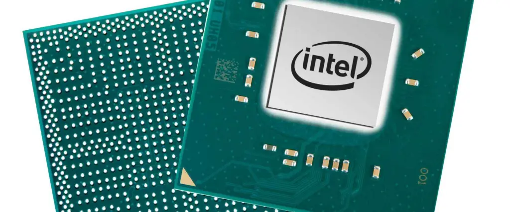
µBGA (Micro Ball Grid Array) Defect Inspection
After the soldering process, the component of BGA can easily be detected. However, the component, equipment, soldering process, and environmental issues may create defects. These defects may include open circuits, cold soldering, short circuits, bridging, loss soldering, and misalignment. Nevertheless, sometimes the BGA solder balls contain defective problems like missing balls and uneven sizes.
The BGA inspection may cause difficulty in judging the high quality of the final product. It is associated with the fact that solder balls of BGA are placed beneath the visual inspection and the chip. This, however, is not able to show the cavities available in the solder joints. Therefore, the inspection demands professional and sophisticated inspection equipment that gives quality results. Such advanced methods include boundary scans, X-ray inspections, and electrical tests.
The traditional ways of electrical testing prove ideal for detecting short and open circuits. Whereas the boundary scan aids in accessing solder joints, there they make a connection which is called boundary connectors. This allows you to inspect short and open circuits over the connected SMD components. The method of boundary scan also allows the testing of invisible and unseen joints more than the electrical tests. Both prove effective in inspecting the electrical performance and conduction of a board. However, they cannot inspect the solder quality. Therefore, you must incorporate other methods with these technologies that help in finding the solder quality as well as the solder present in hidden and invisible joints.
The X-ray machine method carries out other defects that are created during the assembly of BGA PCB. The X-ray inspection eliminates soldering issues like solder balls and pastes bridging. Though, some X-ray machines contain software support that can easily compute gao size in a solder ball. This, however, ensure that the X-ray machine must follow the standard set. A 2D X-ray machine helps in generating 3D images to analyze inner layers, cold soldered joints, blind vias, and vias on the soldered joint of a BGA.
Benefits Of µBGA (Micro Ball Grid Array)
Because of the complex structure of the µBGA package as compared to other surface-mount devices, it possesses a smaller contact length between the pin of the device and the outer world. However, it gives a low impedance and inductance path to each signal. Along with technologies of logic implementation and the advancement of Integrated Circuit semiconductors, it keeps pace and minimizes the loss of signal by enhancing the density of packages and reducing the delay in the packaging process.
The electrical performance of a µBGA represents that it was apple or resistance, inductance, and capacitance of shorter leads. For devices with high- performance, an additional ground plan then minimizes the mutual and self-inductance and crosstalk.
Whereas micro BGAs indicate a major advancement in the packaging of components as they create greater challenges for PCB layout. A general micro or µBGA package comprises a pitch of 0.4mm, while the advanced clear-pitch BGA comes in smaller pitches like 0.25mm and 0.3mm. Designers of PCB need to find easier methods and solutions for pin routing with a BGA pitch of 0.4mm; otherwise, it may result in routing complications. Eventually, those complications result in increasing the layer count along with high requirements of the fabrication process. This implies that before using a design for a microBGA package, designers need to analyze the details of the device of microBGA carefully. It also ensures that the pin pitch of a ball allows the routing of all traces without using unwanted special requirements of manufacturing. Additionally, this process can be carried out within the desired layer counts.
However, this shows that designers want to optimize the layer count needed for routing packages of greater pin count without importing their performance. Moreover, the pin grounding and assignment of a microBGA may be easily modified to allow efficient routing along with an optimal number of board layers.
NSMD & SMD Pads Of µBGA (Micro Ball Grid Array)

The manufacturer of chips has detailed information sheets which consist of land patterns. BGA pads typically have two kinds of surface patterns. Solder Mask-Defined or SMD pads and Non-Solder Mask-Defined or NSMD pads.
The NSMD pads contain openings of solder masks. These openings are larger as compared to the pads. At the same time, the SMD pads contain openings of solder masks. These openings seem smaller as compared to the pads of copper. The majority of suppliers suggest using NSMD as it gives stronger control of the artwork registration of copper than the process of solder mask positional tolerance. Therefore, this becomes even more essential when PCB designers work with clear-pitch components such as the µBGA package.
µBGA (Micro Ball Grid Array) In PCB Design
The routing or fanout technique considers a few aspects like surface diameter, ball pitch, via type, size of the pad, layer count, trace spacing or width, and the number of input/output pins needed to get away from micro BGA.
A conventional dog-bone routing pattern does not seem appropriate for the micro BGA. This enhances the need for buried/blind via or via-in-pad. The method of via-in-pad puts a direct via beneath the contact pads of the device. These vias are filled with either conductive copper or other conductive material like silver. Thus providing a flat surface. This improves the routing and gives high density to the components.
It clearly shows that the traditional method of BGA routing does not work here. This implies that the manufacturer has to use either buried/blind vias or via-in-pad or maybe both. However, do not use buried or blind vias if you really want to make the manufacturing process of PCB cost-effective. Although, it is truly based on the size of the micro BGA and the arrangement of pins.
The package of micro BGA enhances the complexity of the design. The narrow pitch of the package creates various challenges in the design of PCB because of placing a larger number of component pins within the design of a compact area than a traditional BGA. In the same manner, the fabrication of the board has to go through advanced techniques and methods, which increases the cost. The PCB manufacturers need to create a simple fabrication process of a PCB for such types of components and must consider placing pitch components.
The Micro BGA offers various physical and electrical benefits. Moreover, like every other technology, a micro BGA also does not come without issues. For instance, no one can find expertise like micro BGA easily or commonly. The method of rework gets more complicated, while the reliability of the solder joint is even more critical. Additionally, voiding is becoming a fast-growing issue, whereas the assembly inspection of micro BGA also gets difficult.