Introduction
The Xilinx XA Spartan-3A Automotive (XA) FPGA family brings low-cost, reliability-optimized programmable logic to automotive applications. Within this family, the XA3SD1800A-4CSG484Q provides a balance of logic density, features, and package size suitable for body electronics, instrumentation, and engine management systems.
In this article, we will explore the key capabilities and specifications of the XA3SD1800A from its datasheet and reference manual. We’ll examine the programmable logic, hard IP blocks, I/O, reliability, and other relevant details for automotive usage.
XA3SD1800A FPGA Characteristics

The Xilinx XA3SD1800A sits towards the higher end of the XA Spartan-3A family with these high-level characteristics:
Programmable Logic
- 176,592 logic gates
- 1.47 Mb block RAM
- 20 DSP slices
I/O Count
- 484 I/O pins
- Support for common I/O standards
Hard IP Blocks
- PCI Express Endpoint
- Gigabit Ethernet MAC
- Digital Clock Manager blocks
Package
- 23×23 mm 484-pin fine-pitch BGA
- Supported from -40C to +125C
This provides ample logic and routing for reasonably complex automotive applications.
FPGA Logic Cells
The core FPGA fabric that implements custom logic consists of 176,592 usable gates, organized into:
- Configurable logic blocks (CLBs) each with 4 slices
- Slices containing LUTs and flip-flops
- D-type registers for pipeline stages
- Wide multiplexers for complex logic
- Fast carry logic for arithmetic
The FPGA fabric is built on a 150nm process optimized for automotive reliability and qualification.
Block RAM Resources
For data buffering and memory, the XA3SD1800A contains 1470 Kb of fast block RAM, organized into:
- 65 dual-port 18 Kb blocks
- Can be used as single port 36 Kb RAMs
- True dual port capability with simultaneous access
- Configurable aspect ratios for depth vs width
Block RAM enables on-chip data manipulation without external memories.
DSP Slices
For high-speed arithmetic processing, the FPGA includes 20 dedicated DSP slices, each providing:
- 25 x 18 bit signed multiply with 48-bit accumulate
- Optional adder feeding back into multiplier input
- Cascading allows deeper bit precision
- Pipelining and shifting capabilities
This enables efficient implementation of filters, fast transforms, and signal processing.
PCI Express Block
The integrated PCIe block provides a single x1 lane endpoint, with:
- PCIe 1.1 compliant interface at 2.5 Gbps
- Transaction layer and data link layer support
- Supports serial transceivers up to 3.125 Gbps
- Provides high speed interconnect without consuming FPGA resources
Gigabit Ethernet Blocks
Two Ethernet MAC blocks support 10/100/1000 Mbps operation with:
- 1500 byte jumbo frame support
- Simplex, duplex, and autonegotiation modes
- RGMII interface to external PHY
- Scatter-gather DMA
- Statistics counter registers
Clock Management
Six digital clock managers (DCMs) provide:
- Input clock synthesis up to 500 MHz
- Zero-delay buffering on clock nets
- Precision clock deskew, division, and phase alignment
Multiple low-skew global clock networks distribute and route clocks to logic areas with precise matching.
XA3SD1800A Packaging
The XA3SD1800A is available in FCBGA484 package:
- 23x23mm body, 1mm ball pitch
- Supported -40C to +125C temperature range
- Pb-free , RoHS compliant
The high density 1mm pitch provides sufficient routing escape. Rugged specs allow under-hood automotive operation.
XA Automotive Qualification
Additional automotive focused qualification includes:
- AEC-Q100 testing verification
- Production monitoring and change control
- Extended temperature range
- Enhanced material screening and traceability
- Reduced defects and fault tolerance
- ASIL ready capabilities
Ensuring suitability for automotive deployment.
Development Tools
Xilinx provides multiple design tool options:
- ISE Design Suite for RTL synthesis and Place and Route
- EDK for embedded development
- Chipscope analysis tools
- Core generator IP library
- Reference designs
These represent a mature toolchain for developing on XA3SD1800A devices.
Conclusion
With its blend of programmable logic, hard IP blocks, automotive-grade qualification, and medium density, the Xilinx XA3SD1800A-4CSG484Q FPGA provides a proven option for cost-optimized automotive applications. The integrated PCIe, Ethernet, memory, and DSP make it well suited for body electronics, gateways, instrumentation, and control systems in next-generation vehicles.
Frequently Asked Questions
Q: How does the XA3SD1800A compare to newer Xilinx Automotive FPGA families?
A: Newer families like XA7 and XA3S provide higher logic density, performance, and features by leveraging smaller process nodes. But XA3SD offers a cost-optimized legacy option.
Q: What is the typical static power consumption for the XA3SD1800A FPGA?
A: Static power depends on configuration but is typically 130-200mW. Active power peaks around 1.5W for complex designs.
Q: What is the maximum supported transceiver speed in the XA3SD1800A?
A: The integrated PCIe block supports Gen 1 speeds up to 2.5Gbps. GTX transceivers can reach up to 3.75Gbps using external SERDES.
Q: Does the XA3SD1800A support functional safety features?
A: While not ASIL-certified, the XA3SD family does provide SEU mitigation and other features to help meet ISO26262 requirements.
Q: What configuration bitstream storage is recommended for the XA3SD1800A?
A: An 8Mb SPI flash provides room for multiple bitstreams. Larger memories provide storage for more FPGA images.
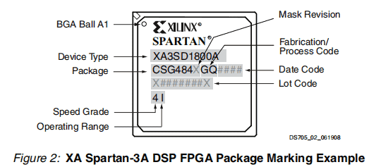
XA devices are available in both extended-temperature Q-Grade (–40°C to +125°C TJ) and I-Grade (–40°C to +100°C TJ) and are qualified to the industry recognized AEC-Q100 standard.
The XA Spartan-3A DSP family builds on the success of the earlier XA Spartan-3E and XA Spartan-3 FPGA families by adding hardened DSP MACs with pre-adders, significantly increasing the throughput and performance of this low-cost family. These XA Spartan-3A DSP family enhancements, combined with proven 90 nm process technology, deliver more functionality and bandwidth per dollar than ever before, setting the new standard in the programmable logic industry.
Because of their exceptionally low cost, XA Spartan-3A DSP FPGAs are ideally suited to a wide range of automotive electronics applications, including infotainment, driver information, and driver assistance modules.
The XA Spartan-3A DSP family is a superior alternative to mask programmed ASICs. FPGA components avoid the high initial mask set costs and lengthy development cycles, while also permitting design upgrades in the field with no hardware replacement necessary because of its inherent programmability, an impossibility with conventional ASICs and ASSPs with their inflexible architecture.

Key Features
1. 250 MHz DSP48A slices using XtremeDSP™ solution
2. Dedicated 18-bit by 18-bit multiplier
3. Available pipeline stages for enhanced performance of at least 250 MHz in the standard -4 speed grade
4. 48-bit accumulator for multiply-accumulate (MAC) operation
5. Integrated adder for complex multiply or multiply-add operation
6. Integrated 18-bit pre-adder
7. Optional cascaded Multiply or MAC
8. Dual-range VCCAUX supply simplifies 3.3V-only design
9. Suspend and Hibernate modes reduce system power
10. Multi-voltage, multi-standard SelectIO™ interface pins
11. Up to 519 I/O pins or 227 differential signal pairs
12. LVCMOS, LVTTL, HSTL, and SSTL single-ended I/O
13. 3V, 2.5V, 1.8V, 1.5V, and 1.2V signaling
14. Selectable output drive, up to 24 mA per pin
15. QUIETIO standard reduces I/O switching noise
16. Full 3.3V ± 10% compatibility and hot-swap compliance
17. 622+ Mb/s data transfer rate per differential I/O
18. LVDS, RSDS, mini-LVDS, HSTL/SSTL differential I/O with integrated differential termination resistors
19. Enhanced Double Data Rate (DDR) support
20. DDR/DDR2 SDRAM support up to 266 Mb/s
21. Fully compliant 32-bit, 33 MHz PCI® technology support
22. Abundant, flexible logic resources
23. Densities up to 53,712 logic cells, including optional shift register
24. Efficient wide multiplexers, wide logic
25. Fast look-ahead carry logic
26. IEEE 1149.1/1532 JTAG programming/debug port
27. Hierarchical SelectRAM™ memory architecture
28. Up to 2,268 Kbits of fast block RAM with byte write enables for processor applications
29. Up to 373 Kbits of efficient distributed RAM
30. Registered outputs on the block RAM with operation of at least 280 MHz in the standard -4 speed grade
31. Eight Digital Clock Managers (DCMs)
32. Clock skew elimination (delay locked loop)
33. Frequency synthesis, multiplication, division
34. High-resolution phase shifting
35. Wide frequency range (5 MHz to over 320 MHz)
36. Eight low-skew global clock networks, eight additional clocks per half device, plus abundant low-skew routing
37. Configuration interface to industry-standard PROMs
38. Low-cost, space-saving SPI serial Flash PROM
39. x8 or x8/x16 parallel NOR Flash PROM
40. Unique Device DNA identifier for design authentication
41. Complete Xilinx ISE® and WebPACK™ software support plus Spartan-3A DSP FPGA Starter Kit
42. MicroBlaze™ and PicoBlaze™ embedded processor cores
43. BGA packaging, Pb-free only