Printed Circuit Boards (PCBs) are the backbone of modern electronics. While many opt for professional PCB manufacturing services, there’s a growing trend among hobbyists and small-scale manufacturers to create PCBs using milling techniques. This article will guide you through the process of making PCB milling boards, offering a comprehensive, step-by-step approach that both beginners and experienced makers can follow.
Understanding PCB Milling
What is PCB Milling?
PCB milling is a subtractive manufacturing process where a CNC (Computer Numerical Control) machine removes copper from a copper-clad board to create the desired circuit pattern. This method offers several advantages over traditional etching techniques, including:
- Faster prototyping
- No hazardous chemicals
- Ability to create double-sided boards
- Precision in creating fine traces and pads
Tools and Materials Needed
Before we dive into the process, let’s review the essential tools and materials you’ll need:
| Parameter | Recommendation |
| Feed rate | 100-200 mm/min for copper, 50-100 mm/min for drilling |
| Plunge rate | 30-50 mm/min |
| Depth of cut | 0.1-0.2 mm for isolation routing, full depth for drilling |
| Tool change positions | Safe coordinates for bit changes |
Step 1: Designing Your PCB

Choosing PCB Design Software
The first step in creating your PCB is designing it using appropriate software. Some popular options include:
- KiCad (open-source and free)
- Eagle (free for hobbyist use)
- Altium Designer (professional-grade, paid)
- Fusion 360 (free for personal use, includes CAM features)
Design Considerations for Milling
When designing your PCB for milling, keep these factors in mind:
- Trace width: Aim for wider traces than you might use with professional manufacturing.
- Clearance: Leave more space between traces to account for milling tolerances.
- Component placement: Consider the milling bit size when placing components.
- Edge cuts: Include mounting holes and board outline in your design.
Step 2: Preparing the Design for Milling
Exporting Gerber Files
Once your design is complete, export it as Gerber files. These files contain the information needed to manufacture your PCB. Typically, you’ll need:
- Top copper layer
- Bottom copper layer (if double-sided)
- Drill file
- Board outline
Generating G-code
Next, convert your Gerber files into G-code, which your CNC machine can understand. Software options for this step include:
- FlatCAM
- pcb2gcode
- CAM processors built into some PCB design software
When generating G-code, consider these settings:
| Issue | Possible Cause | Solution |
| Incomplete cuts | Incorrect depth setting | Adjust Z-axis zero or increase cutting depth |
| Traces lifting | Over-milling or board not secure | Reduce cutting depth or improve board fixation |
| Drill holes misaligned | Machine not properly zeroed | Re-zero the machine and verify G-code |
| Rough edges | Feed rate too high | Reduce feed rate in G-code |
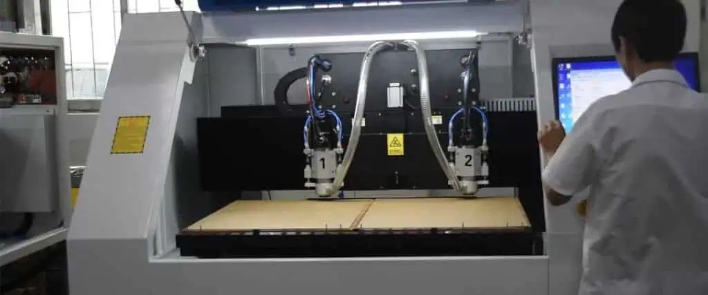
Step 3: Setting Up the CNC Machine
Choosing the Right Bits
Select appropriate milling bits for your project:
- Isolation routing: 0.1mm – 0.3mm V-shaped engraving bit
- Drilling: 0.8mm – 1.0mm drill bit
- Board outline: 1.5mm – 2.0mm flat end mill
Preparing the Copper-Clad Board
- Cut the copper-clad board to size, leaving extra margin around your design.
- Clean the surface with isopropyl alcohol and a lint-free cloth.
- Secure the board to the CNC machine’s bed using double-sided tape or a vacuum table.
Zeroing the Machine
Proper zeroing is crucial for accurate milling:
- Home all axes of your CNC machine.
- Use a probe or manually set the Z-axis zero point on the copper surface.
- Set the X and Y zero points at a corner of your board.
Step 4: Milling the PCB
Isolation Routing
- Load the G-code for copper removal into your CNC control software.
- Start with a test run without the bit touching the board to verify the path.
- Run the isolation routing program, monitoring closely for any issues.
Drilling
- Change to the appropriate drill bit.
- Load the drilling G-code.
- Run the drilling program.
Cutting the Board Outline
- Switch to the larger end mill for the board outline.
- Load and run the outline cutting G-code.
- Be prepared to catch the board as it’s cut free from the stock material.
Step 5: Post-Processing
Cleaning the Board
- Remove any debris with compressed air or a soft brush.
- Clean the board again with isopropyl alcohol to remove any oils or residue.
Inspection and Testing
- Visually inspect the board for any shorts or incomplete cuts.
- Use a multimeter to check for continuity and shorts between traces.
- If necessary, use a fine file or knife to clean up any problem areas.
Applying Solder Mask (Optional)
For added protection and a professional look:
- Apply liquid solder mask to areas between traces.
- Cure the solder mask according to the product instructions.
Step 6: Component Assembly
Soldering Components
- Begin with SMD (Surface Mount Device) components if your design includes them.
- Move on to through-hole components.
- Double-check component orientation and polarity before soldering.
Final Testing
- Perform a visual inspection of all solder joints.
- Use a multimeter to check for shorts and proper connections.
- If possible, run a functional test of your circuit.
Troubleshooting Common Issues
IssuePossible CauseSolutionIncomplete cutsIncorrect depth settingAdjust Z-axis zero or increase cutting depthTraces liftingOver-milling or board not secureReduce cutting depth or improve board fixationDrill holes misalignedMachine not properly zeroedRe-zero the machine and verify G-codeRough edgesFeed rate too highReduce feed rate in G-code
Conclusion
Creating PCB milling boards is a rewarding process that offers rapid prototyping capabilities for electronics enthusiasts. While it requires some initial investment in equipment and a learning curve, the ability to produce custom PCBs quickly and without chemicals is invaluable. As you gain experience, you’ll be able to create increasingly complex designs and refine your milling techniques.
FAQ
Q1: What’s the smallest trace width I can reliably mill?
A1: With a well-tuned CNC machine and a 0.1mm V-bit, you can achieve trace widths down to about 0.2mm. However, for better reliability, especially when starting out, aim for trace widths of 0.3mm or larger.
Q2: Can I mill double-sided PCBs?
A2: Yes, you can mill double-sided PCBs. This requires careful alignment when flipping the board and potentially the use of alignment pins. Some CNC software offers features to assist with double-sided milling.
Q3: How long does it take to mill a typical PCB?
A3: The time varies greatly depending on the complexity of your design and the size of the board. A simple, single-sided 5cm x 5cm board might take 30-60 minutes to mill, while a complex double-sided board could take several hours.
Q4: Is PCB milling suitable for mass production?
A4: PCB milling is best suited for prototyping and small-scale production. For larger quantities (typically more than 10-20 boards), traditional PCB manufacturing methods become more time and cost-effective.
Q5: What’s the main advantage of milled PCBs over etched PCBs?
A5: The main advantages of milled PCBs are the absence of hazardous chemicals, faster turnaround time for prototypes, and the ability to easily make design changes on the fly. Milling also allows for more precise control over trace impedance, which can be crucial for high-frequency circuits.