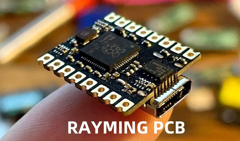
The Raspberry Pi RP2040 microcontroller (MCU) has gained popularity among hobbyists and professionals alike due to its affordability and versatility. Designing a minimalistic printed circuit board (PCB) for this MCU can be a daunting task, especially when incorporating a buck (step-down) converter for efficient power management. In this comprehensive article, we will explore the step-by-step process of creating a minimalistic PCB design that includes a buck converter for the Raspberry Pi RP2040 MCU.

Understanding the Raspberry Pi RP2040 MCU
Before diving into the PCB design process, it’s essential to understand the Raspberry Pi RP2040 MCU and its capabilities.
Features of the RP2040 MCU
- Dual-core Arm Cortex-M0+ processor clocked at 133 MHz
- 264kB of SRAM
- 30 multi-purpose GPIO pins
- Support for various peripherals, including UART, SPI, I2C, and more
- Programmable in C/C++ or MicroPython
Designing the Minimalistic PCB

The design process of a minimalistic PCB involves several steps, from selecting the necessary components to creating the PCB layout. Here’s a step-by-step guide to help you through the process.
Step 1: Component Selection
The first step in designing a PCB is to select the appropriate components. For our minimalistic design, we’ll need the following components:
- Raspberry Pi RP2040 MCU
- Buck (step-down) converter
- Decoupling capacitors
- Resistors (if required)
- Connectors (e.g., USB, GPIO headers)
Step 2: Schematic Design
Once you’ve selected the components, the next step is to create the schematic design. This involves creating a visual representation of the electrical connections between the components. You can use a schematic capture software like KiCad or Eagle for this task.
Schematic Design for the RP2040 MCU
The schematic design for the RP2040 MCU should include the following:
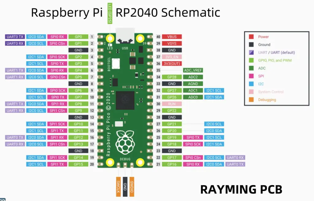
- Power supply connections (VCC and GND)
- GPIO pins
- Communication interfaces (UART, SPI, I2C)
- Reset and boot pins
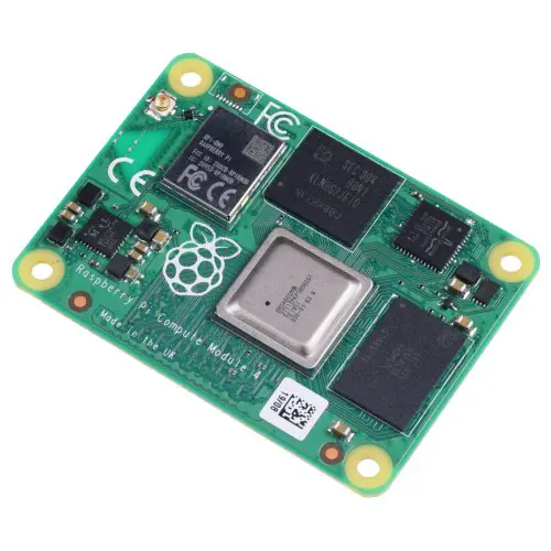
Raspberry Pi Compute Module 4 – 8GB RAM, 32GB eMMC, 2.4/5.0GHz Wi-Fi & Bluetooth 5.0
This version of the Raspberry Pi Compute Module 4 includes a high-performance 64-bit quad-core processor, 8GB LPDDR4 RAM, 32GB eMMC, dual-display support at resolutions up to 4K, hardware video decode at up to 4Kp60, Gigabit Ethernet, USB 2.0, dual camera interfaces, PCIe Gen 2 x1 interface, and dual-band 2.4/5.0GHz wireless LAN and Bluetooth 5.0.
Schematic Design for the Buck Converter
The schematic design for the buck converter should include:
- Input voltage (e.g., 5V from USB)
- Output voltage (e.g., 3.3V for the RP2040)
- Feedback and compensation components
- Output capacitors
Step 3: PCB Layout
After creating the schematic design, the next step is to design the PCB layout. This involves arranging the components and routing the traces on the PCB.
PCB Layout Considerations
When designing the PCB layout, consider the following factors:
- Component placement: Arrange the components in a logical and space-efficient manner.
- Trace routing: Route the traces carefully to minimize interference and signal integrity issues.
- Ground plane: Include a ground plane for better signal integrity and heat dissipation.
- Thermal management: Ensure proper heat dissipation for the buck converter and other heat-generating components.
PCB Layout for the RP2040 MCU
The PCB layout for the RP2040 MCU should include:
- Footprint for the RP2040 MCU
- GPIO pins and communication interfaces
- Decoupling capacitors close to the power pins
PCB Layout for the Buck Converter

The PCB layout for the buck converter should include:
- Footprint for the buck converter IC
- Input and output capacitors
- Feedback and compensation components
- Proper grounding and heat dissipation
Step 4: Design Review and Verification
Before finalizing the PCB design, it’s crucial to review and verify the design. This includes:
- Checking for any design rule violations
- Verifying the component placement and trace routing
- Performing electrical rule checks (ERC)
- Simulating the design (if possible) to identify potential issues
Step 5: PCB Fabrication and Assembly
Once you’ve verified the PCB design, you can proceed with the fabrication and assembly process. You can either fabricate the PCB yourself using a PCB milling machine or outsource the fabrication to a PCB manufacturer.
After receiving the fabricated PCB, you’ll need to assemble the components onto the board. This can be done manually or with the help of an automated assembly process, depending on the complexity of the design and the available resources.
Frequently Asked Questions (FAQ)
Q1: Why do we need a buck converter in the PCB design?
A buck converter is necessary to step down the input voltage (e.g., 5V from USB) to the required operating voltage of the RP2040 MCU (e.g., 3.3V). By incorporating a buck converter, we can ensure efficient power management and prevent voltage overstress on the MCU.
Q2: Can I use a different microcontroller instead of the RP2040?
Yes, you can adapt the PCB design to accommodate different microcontrollers. However, you’ll need to adjust the schematic and layout according to the pinout and specifications of the chosen microcontroller.
Q3: How do I program the RP2040 MCU?
The RP2040 MCU can be programmed using various methods, including:
- C/C++ programming using the Raspberry Pi Pico SDK
- MicroPython programming
- Arduino IDE (with additional libraries and configurations)
The programming method you choose will depend on your project requirements and familiarity with the programming language or environment.
Q4: What are the advantages of using a minimalistic PCB design?
A minimalistic PCB design offers several advantages, including:
- Cost-effectiveness: Fewer components and a smaller PCB result in lower manufacturing costs.
- Simplicity: A minimalistic design is easier to understand, troubleshoot, and maintain.
- Portability: A compact PCB design allows for easy integration into various projects and applications.
Q5: Can I add additional components to the PCB design?
Yes, you can certainly add additional components to the PCB design based on your project requirements. However, keep in mind that adding more components may increase the complexity and size of the PCB design, which could potentially negate the benefits of a minimalistic approach.
Conclusion
Designing a minimalistic PCB for the Raspberry Pi RP2040 MCU, including a buck converter, can be a rewarding and educational experience. By following the steps outlined in this article, you’ll be able to create a compact and efficient PCB design that meets your project requirements. Remember to carefully consider component selection, schematic design, PCB layout, and design verification to ensure a successful PCB implementation.

