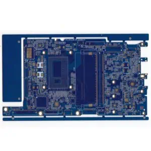
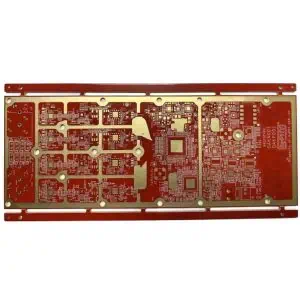
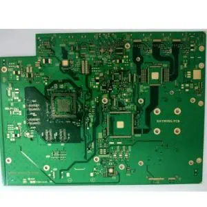
Maximize PCB Real Estate with Advanced Via-in-Pad Manufacturing
Via-in-Pad PCB technology represents a breakthrough in high-density circuit board design, allowing designers to place vias directly underneath component pads rather than routing them around components. This innovative approach dramatically reduces board size while maintaining signal integrity and manufacturing reliability.
Key Features
Space Optimization: Eliminate the need for additional routing channels by positioning vias directly within component footprints, reducing overall PCB dimensions by up to 30% compared to traditional designs.
Enhanced Signal Integrity: Minimize trace lengths and reduce parasitic effects through direct connections, resulting in improved electrical performance and reduced electromagnetic interference.
High-Density Integration: Enable tighter component placement and support for advanced packaging technologies including BGAs, CSPs, and high pin-count processors.
Manufacturing Excellence: Utilize specialized via filling and planarization processes to ensure reliable solder joints and eliminate voiding issues that can compromise component attachment.
Technical Specifications
- Via Size Range: 0.1mm to 0.3mm diameter
- Fill Materials: Conductive epoxy, copper plating, or resin plug options
- Surface Planarity: ±25 microns across pad surface
- Layer Count: Compatible with 4-32 layer constructions
- Minimum Spacing: 0.15mm via-to-via clearance
Applications
Ideal for space-constrained designs in mobile devices, wearables, automotive electronics, aerospace systems, and high-speed digital applications where board real estate is at a premium.
Transform your next design with Via-in-Pad technology and achieve unprecedented miniaturization without compromising performance.