A smart digital AVO (Ampere, Volt, Ohm) meter represents a significant advancement over traditional analog multimeters, offering enhanced accuracy, data logging capabilities, and digital connectivity features. The printed circuit board (PCB) serves as the backbone of this sophisticated instrument, requiring careful design considerations to ensure optimal performance and reliability.
PCB Design Fundamentals
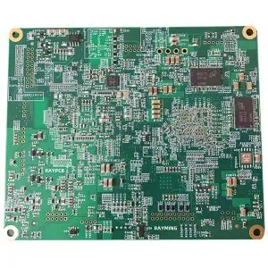
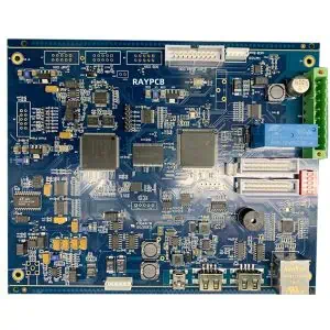
The PCB design for a smart digital AVO meter must accommodate multiple critical components including analog-to-digital converters (ADCs), microcontrollers, precision voltage references, current sensing circuits, and display drivers. The layout requires meticulous attention to signal integrity, particularly for low-level analog signals that can be easily corrupted by digital switching noise.
Ground plane design is paramount in AVO meter PCBs. Implementing separate analog and digital ground planes, connected at a single point, minimizes ground loops and reduces measurement errors. The analog front-end circuitry should be isolated from high-frequency digital switching circuits through careful component placement and strategic use of guard traces.
Power supply design within the PCB must provide stable, low-noise voltage rails for sensitive analog components. Multiple voltage regulators may be required to supply different circuit sections, with particular attention paid to the voltage reference circuits that directly impact measurement accuracy. Decoupling capacitors must be strategically placed near power pins to minimize supply noise.
Component Integration and Protection
Smart AVO meters require robust input protection circuits to handle overvoltage conditions and prevent damage from incorrect connections. The PCB must accommodate high-voltage MOSFETs, current limiting resistors, and transient voltage suppressors. These protection circuits must be designed to respond quickly while maintaining measurement accuracy under normal operating conditions.
The microcontroller section of the PCB handles measurement processing, user interface control, and communication functions. Modern smart meters often include wireless connectivity (WiFi, Bluetooth) or USB interfaces, requiring dedicated circuit areas with proper impedance control for high-frequency signals. Antenna placement and ground plane considerations become critical for wireless-enabled designs.
Manufacturing Considerations
PCB manufacturing for precision instruments demands tight tolerances and high-quality materials. FR-4 substrate with controlled dielectric properties ensures consistent impedance characteristics. The copper thickness must be carefully specified to handle expected current levels while maintaining trace resistance accuracy for current sensing applications.
Via placement and sizing significantly impact signal integrity in multi-layer designs. Thermal vias may be necessary under high-power components like voltage regulators or current sensing resistors. The solder mask design must accommodate precision components with fine-pitch packages while providing adequate solder joint reliability.
Testing and Quality Assurance
Manufacturing testing protocols for AVO meter PCBs typically include in-circuit testing (ICT) to verify component placement and basic functionality. Functional testing must validate measurement accuracy across the full range of voltage, current, and resistance measurements. Automated test equipment (ATE) can perform rapid calibration verification and ensure each unit meets specified accuracy requirements.
Environmental testing becomes crucial for portable instruments, requiring PCB designs that withstand temperature cycling, humidity exposure, and mechanical stress. The choice of components, solder alloys, and conformal coatings all contribute to long-term reliability in challenging operating environments.
The evolution toward smart digital AVO meters continues to drive innovation in PCB design, incorporating advanced features like touchscreen interfaces, data