Transform your electronic concepts into production-ready circuit boards with our comprehensive PCB design services. We bridge the gap between your schematic designs and manufacturable PCB layouts, ensuring optimal performance, reliability, and cost-effectiveness.
What We Deliver
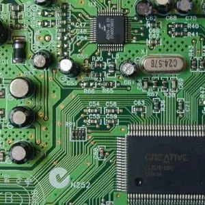
Our experienced PCB designers take your schematic files and component specifications to create complete board layouts ready for fabrication. We handle every aspect of the design process, from component placement optimization to advanced routing strategies, delivering industry-standard Gerber files and comprehensive documentation packages.
Key Service Features
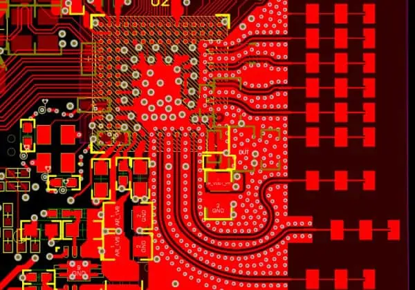
Complete Design Translation – We convert your schematics into fully routed PCB layouts while maintaining signal integrity and design intent. Our team works with popular EDA tools including Altium Designer, KiCad, Eagle, and Cadence.
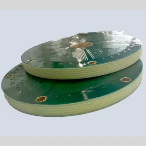
Multi-Layer Expertise – From simple 2-layer boards to complex 12+ layer designs, we optimize stackup configurations for your specific requirements, whether for high-speed digital, RF/microwave, or mixed-signal applications.
Design Rule Compliance – Every layout adheres to your manufacturer’s specifications and industry standards, including IPC guidelines, ensuring high yield rates and reliable production.
Signal Integrity Focus – We implement proper impedance control, differential pair routing, and EMI/EMC considerations to ensure your circuits perform as designed, especially critical for high-frequency and sensitive analog circuits.
Design Process
Our structured approach begins with thorough schematic review and component selection verification. We create optimized component placement considering thermal management, mechanical constraints, and assembly requirements. Advanced routing techniques ensure clean signal paths while minimizing crosstalk and interference. Each design undergoes comprehensive DRC checks and design reviews before final deliverable preparation.
Deliverables Package
You receive complete Gerber files, drill files, pick-and-place data, bill of materials, assembly drawings, and fabrication notes. We also provide 3D renderings and optional design documentation for manufacturing and assembly partners.
Typical Turnaround: 3-10 business days depending on complexity Revisions: Up to 2 rounds of revisions included Support: Post-delivery technical support through prototype phase
Ready to transform your schematic into a professional PCB layout? Contact us with your design files for a detailed quote and timeline.