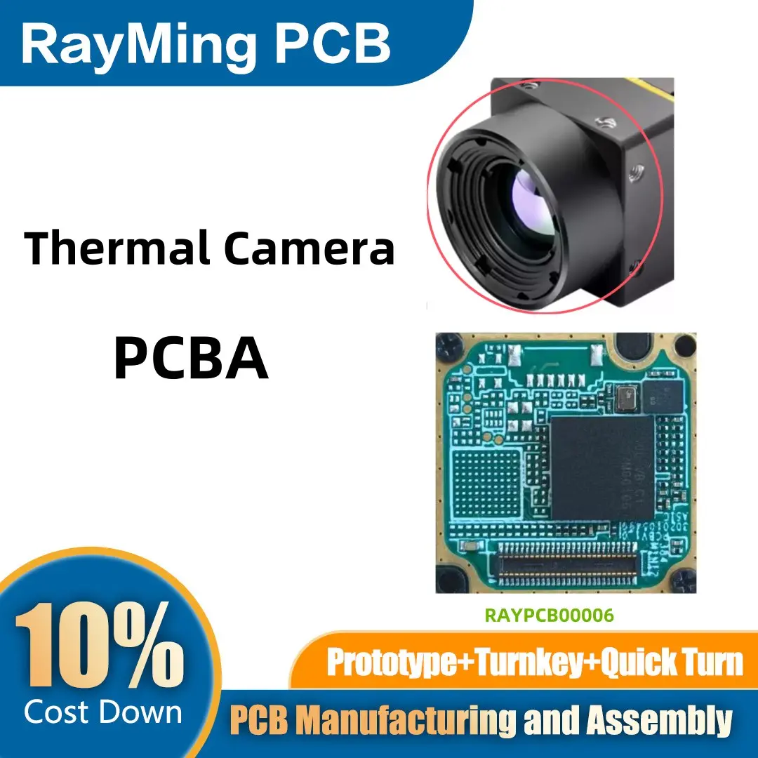
Thermal cameras are advanced imaging devices that detect infrared radiation to create visual representations of temperature differences in a scene. These devices are widely used in applications such as security surveillance, industrial inspection, medical diagnostics, and firefighting. The Printed Circuit Board (PCB) is a critical component of a thermal camera, as it houses the electronic circuitry that processes infrared signals, controls the camera’s functions, and interfaces with other systems. The manufacturing and assembly of a thermal camera PCB require precision, adherence to high-quality standards, and specialized techniques to ensure optimal performance and reliability.
1. Design and Material Selection
The design of a thermal camera PCB begins with a detailed understanding of the camera’s requirements, including signal processing, power management, and thermal imaging sensor integration. Key considerations during the design phase include:
- High-Frequency Signal Integrity: Thermal cameras rely on high-frequency signals to process infrared data. The PCB layout must minimize signal loss and interference by using controlled impedance traces and proper grounding techniques.
- Thermal Management: Thermal cameras generate heat during operation, which can affect performance. The PCB design must incorporate thermal vias, heat sinks, and proper component placement to dissipate heat effectively.
- Material Selection: The PCB substrate material must have excellent thermal conductivity and stability. Materials like FR-4 with high thermal performance or specialized substrates such as ceramic or metal-core PCBs are often used to handle the heat generated by the camera’s components.
- Component Integration: Thermal cameras require specialized components, such as infrared sensors, microcontrollers, and analog-to-digital converters (ADCs). These components must be carefully selected and placed to ensure optimal performance and compatibility with the PCB design.
2. PCB Manufacturing
The manufacturing process for a thermal camera PCB involves several steps to create a high-quality board capable of handling the camera’s demanding requirements:
- Layer Stackup: Thermal camera PCBs often use multi-layer designs to accommodate complex circuitry and ensure signal integrity. The layer stackup is carefully planned to separate high-frequency signals, power planes, and ground planes.
- Precision Drilling and Etching: High-precision drilling machines create vias and through-holes for component mounting and inter-layer connections. Copper layers are etched to form the circuit traces, with tight tolerances to ensure accuracy.
- Surface Finish: A suitable surface finish, such as ENIG (Electroless Nickel Immersion Gold) or HASL (Hot Air Solder Leveling), is applied to protect the copper traces and ensure reliable solderability.
- Quality Inspection: Automated Optical Inspection (AOI) and X-ray inspection are used to detect defects such as shorts, opens, or misaligned traces. These inspections ensure the PCB meets the required specifications before assembly.
3. PCB Assembly
The assembly process for a thermal camera PCB involves mounting and soldering components onto the board. This process requires precision and attention to detail to ensure the functionality and reliability of the final product:
- SMT (Surface Mount Technology): Most components, such as resistors, capacitors, and integrated circuits, are mounted using SMT. Automated pick-and-place machines accurately position components on the PCB, followed by reflow soldering to create strong electrical connections.
- Through-Hole Assembly: Larger components, such as connectors or power modules, may require through-hole assembly. These components are manually or automatically inserted and soldered using wave soldering techniques.
- Infrared Sensor Integration: The thermal imaging sensor is a critical component of the camera. It is carefully mounted and aligned to ensure accurate detection of infrared radiation. Specialized soldering techniques may be required to handle the sensor’s sensitivity to heat and static electricity.
- Conformal Coating: To protect the PCB from environmental factors such as moisture, dust, and temperature fluctuations, a conformal coating is applied. This coating also enhances the board’s durability in harsh operating conditions.
4. Testing and Validation
After assembly, the thermal camera PCB undergoes rigorous testing to ensure it meets performance and reliability standards:
- Functional Testing: The PCB is tested to verify its ability to process infrared signals, control camera functions, and interface with other systems.
- Thermal Testing: The board is subjected to thermal cycling tests to ensure it can operate reliably under varying temperature conditions.
- EMC Testing: Electromagnetic compatibility testing ensures the PCB does not emit excessive electromagnetic interference and is immune to external interference.