Advanced High-Performance Circuit Solutions for RF Applications
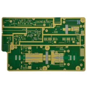
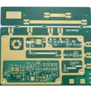
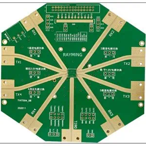
Our Multilayer RF PCBs are engineered for demanding high-frequency applications where signal integrity, minimal loss, and electromagnetic compatibility are critical. These specialized printed circuit boards deliver exceptional performance across a wide frequency spectrum, making them ideal for telecommunications, aerospace, defense, and advanced electronic systems.
Key Features
Superior High-Frequency Performance
- Optimized for frequencies ranging from MHz to GHz applications
- Ultra-low dielectric loss materials minimize signal attenuation
- Controlled impedance matching ensures consistent signal transmission
- Exceptional phase stability across temperature variations
Advanced Multilayer Construction
- Multiple copper layers enabling complex routing and ground plane configurations
- Precision-controlled layer stackup for optimal signal isolation
- Integrated shielding layers to minimize electromagnetic interference (EMI)
- Flexible layer count options from 4 to 20+ layers based on application requirements
Premium Materials & Manufacturing
- High-frequency substrates including Rogers, Taconic, and PTFE-based materials
- Low-loss dielectric materials with stable electrical properties
- Precise copper thickness control for consistent impedance
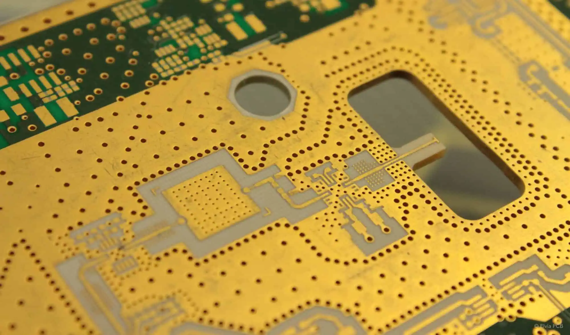
- Advanced via technology including blind, buried, and microvias
Technical Specifications
- Frequency Range: DC to 100+ GHz capability
- Dielectric Constant (Dk): 2.2 to 10.2 (material dependent)
- Loss Tangent: As low as 0.0009
- Copper Weight: 0.5 oz to 2 oz per layer
- Board Thickness: 0.1mm to 6.0mm
- Minimum Trace Width: Down to 25μm (1 mil)
- Via Diameter: As small as 50μm (2 mil)
Applications
- Telecommunications: 5G base stations, antenna systems, microwave transceivers
- Aerospace & Defense: Radar systems, satellite communications, electronic warfare
- Automotive: Advanced driver assistance systems (ADAS), vehicle-to-everything (V2X)
- Medical: High-frequency imaging equipment, therapeutic devices
- Industrial: Test and measurement equipment, RF amplifiers, filters
Quality & Reliability
Our RF PCBs undergo rigorous testing including network analysis, insertion loss measurement, and thermal cycling validation. Each board meets or exceeds industry standards for high-frequency performance, ensuring reliable operation in mission-critical applications.
Available with full design support, impedance control documentation, and comprehensive testing reports to accelerate your product development cycle.