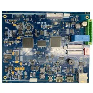
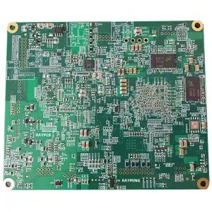
Industrial frequency converters, also known as variable frequency drives (VFDs), play a crucial role in controlling the speed and torque of AC motors in various industrial applications. The heart of these sophisticated devices lies in their Printed Circuit Boards (PCBs), which require careful design and manufacturing to ensure reliability, efficiency, and performance. This article delves into the intricacies of designing and manufacturing PCBs for industrial frequency converters.
PCB Design Considerations
1. Power Stage Design
The power stage is the core of a frequency converter PCB:
- IGBT or MOSFET Selection: Choose high-power semiconductors capable of handling the required voltage and current levels.
- Gate Driver Circuits: Design robust gate driver circuits to ensure proper switching of power semiconductors.
- DC Bus Capacitors: Select and layout capacitors to minimize parasitic inductance and handle high ripple currents.
- Snubber Circuits: Implement snubber circuits to suppress voltage spikes during switching.
2. Control Circuit Design
The control circuit manages the converter’s operation:
- Microcontroller or DSP: Select a processor capable of executing complex control algorithms in real-time.
- Analog-to-Digital Converters (ADCs): Choose high-speed, high-resolution ADCs for accurate current and voltage sensing.
- Isolation: Implement galvanic isolation between power and control circuits using optocouplers or digital isolators.
- Communication Interfaces: Include industrial communication protocols like Modbus, PROFIBUS, or EtherCAT.
3. EMI/EMC Considerations
Electromagnetic Interference (EMI) and Electromagnetic Compatibility (EMC) are critical in industrial environments:
- EMI Filters: Design input and output EMI filters to suppress conducted and radiated emissions.
- Shielding: Implement proper shielding techniques for sensitive circuits and connectors.
- PCB Stack-up: Use a multi-layer PCB design with dedicated power and ground planes for improved EMI performance.
- Component Placement: Separate noisy switching circuits from sensitive analog and digital circuits.
4. Thermal Management
Effective thermal management is crucial for reliability:
- Copper Thickness: Use thicker copper (e.g., 2 oz or 3 oz) for high-current traces.
- Thermal Vias: Implement thermal vias under power components to improve heat dissipation.
- Component Placement: Arrange heat-generating components to optimize airflow and heat distribution.
5. Safety and Protection Features
Incorporate safety features to protect both the converter and connected equipment:
- Overcurrent Protection: Implement fast-acting current sensing and protection circuits.
- Overvoltage Protection: Design circuits to detect and respond to DC bus overvoltage conditions.
- Temperature Monitoring: Include temperature sensors and shutdown circuits to prevent thermal damage.
PCB Manufacturing Process
1. Material Selection
Choose appropriate PCB materials for high-performance and reliability:
- Base Material: Use high-quality FR-4 or consider specialized materials like Rogers or Isola for high-frequency sections.
- Copper Thickness: Select copper weight based on current requirements and thermal considerations.
- Surface Finish: Choose ENIG (Electroless Nickel Immersion Gold) or other suitable finishes for improved solderability and durability.
2. PCB Fabrication
The manufacturing process involves several critical steps:
- Photolithography: Transfer the circuit pattern to the copper-clad laminate with high precision.
- Drilling: Create holes for vias and through-hole components using computer-controlled drilling machines.
- Plating: Apply copper plating to create conductive walls in vias and holes.
- Etching: Remove excess copper to form the final circuit pattern.
- Solder Mask and Silkscreen: Apply solder mask for protection and silkscreen for component identification.
3. Advanced Manufacturing Techniques
Employ advanced techniques for improved performance:
- Controlled Impedance: Maintain specific trace impedances for high-speed signals.
- Buried and Blind Vias: Use these techniques for high-density designs and improved signal integrity.
- Heavy Copper: Implement heavy copper (up to 10 oz) for high-current sections of the PCB.
4. Quality Control and Testing
Implement rigorous quality control measures:
- Automated Optical Inspection (AOI): Detect defects in traces, pads, and solder mask.
- X-ray Inspection: Examine internal layers and hidden solder joints.
- Electrical Testing: Perform flying probe or bed-of-nails testing to verify electrical continuity and isolation.
- Impedance Testing: Verify controlled impedance traces meet design specifications.
PCB Assembly
1. Component Placement
Use advanced pick-and-place machines for precise component placement:
- Fine-Pitch Components: Ensure accurate placement of ICs with fine pitch leads or ball grid arrays.
- Large Power Components: Employ specialized equipment for placing heavy power semiconductors and heatsinks.
2. Soldering Techniques
Apply appropriate soldering methods:
- Reflow Soldering: Use carefully controlled reflow ovens for surface-mount components.
- Selective Soldering: Employ selective soldering for through-hole components in mixed-technology boards.
- Hand Soldering: Perform manual soldering for large power components or any rework needed.
3. Inspection and Testing
Conduct thorough post-assembly inspection and testing: