Product Overview
Professional-grade printed circuit board designed specifically for accurate impedance and transmission line characterization. This specialized test PCB enables engineers to validate signal integrity, measure characteristic impedance, and analyze transmission line performance across various trace geometries and substrate materials.
Key Features
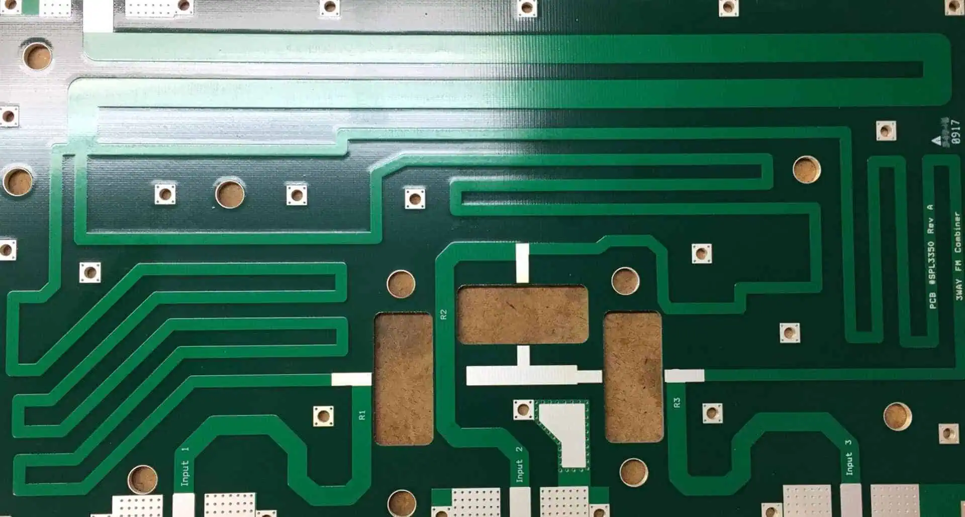
Comprehensive Test Patterns
- Multiple trace widths and spacing configurations for differential and single-ended measurements
- Coplanar waveguide (CPW), microstrip, and stripline test structures
- Via transition test patterns for layer-to-layer impedance verification
- Reference impedance standards (50Ω, 75Ω, 90Ω, 100Ω differential pairs)
High-Precision Design
- Controlled dielectric thickness and material properties
- Gold-plated test pads for reliable probe contact
- Minimal parasitic effects through optimized layout
- Temperature-stable FR-4 or low-loss dielectric substrates available
Measurement Capabilities
- Time Domain Reflectometry (TDR) compatible test points
- S-parameter measurement support up to 20+ GHz
- Crosstalk analysis between adjacent transmission lines
- Return loss and insertion loss characterization
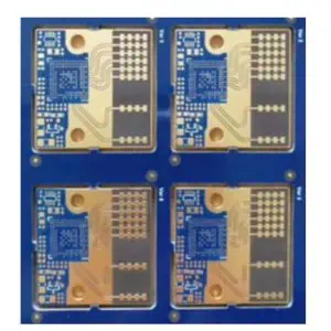
Professional Construction
- 4-layer or 6-layer stackup options
- Precise copper weight control (0.5oz to 2oz)
- Impedance tolerance: ±5% or ±10% as specified
- IPC Class 2 or Class 3 fabrication standards
Applications
- Signal integrity validation for high-speed digital designs
- RF/microwave circuit impedance verification
- PCB fabrication process qualification
- Design rule validation and modeling correlation
- Educational training for transmission line theory
Technical Specifications
- Frequency Range: DC to 20+ GHz
- Substrate Options: FR-4, Rogers, Isola materials
- Board Thickness: 0.8mm to 3.2mm
- Trace Width Range: 50μm to 5mm
- Temperature Range: -40°C to +125°C
- Dimensions: Standard 100mm x 80mm (custom sizes available)
Included Documentation
Complete test procedures, expected measurement results, and correlation guidelines provided with each PCB to ensure accurate and repeatable testing protocols.
Ideal for PCB designers, signal integrity engineers, test labs, and educational institutions requiring precise transmission line characterization and impedance validation.