Transform your electronic designs with cutting-edge HDI PCB technology that delivers unmatched performance in a compact form factor. Our High Density Interconnect PCB design services provide the advanced routing solutions needed for today’s most demanding applications.
What is HDI PCB Design?
HDI PCBs utilize microvias, buried vias, and sequential lamination to achieve significantly higher wiring density than traditional PCBs. This advanced technology enables more connections in smaller spaces through multiple thin dielectric layers and laser-drilled microvias as small as 0.1mm diameter.
Key Features & Capabilities
Advanced Via Technology
- Microvias (0.1-0.15mm diameter) for ultra-fine pitch connections
- Buried and blind vias for optimized layer utilization
- Via-in-pad technology for maximum space efficiency
- Sequential build-up layers for complex routing
High-Density Performance
- Line widths down to 75-100 microns
- Spacing as tight as 75-100 microns
- Component pitch support down to 0.4mm BGA
- Up to 20+ layers with controlled thickness
Superior Signal Integrity
- Reduced electromagnetic interference (EMI)
- Minimized crosstalk through optimized layer stackup
- Controlled impedance for high-speed signals
- Enhanced power distribution networks
Applications
HDI PCB design is essential for:
- Smartphones and tablets
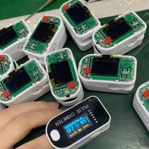
- Wearable devices and IoT sensors
- High-performance computing systems
- Medical devices and implantables
- Aerospace and defense electronics
- 5G communication equipment
- AI and machine learning hardware
Design Benefits
Space Optimization: Achieve 40-60% size reduction compared to conventional PCBs while maintaining full functionality.
Enhanced Performance: Superior electrical characteristics with reduced parasitic effects and improved signal propagation.
Increased Reliability: Shorter connection paths reduce failure points and improve overall system reliability.
Cost Efficiency: Despite higher initial costs, HDI designs often reduce total system cost through miniaturization and improved yields.
Our HDI Design Process
Our experienced engineers utilize industry-leading CAD tools and follow IPC-2226 standards to deliver optimized HDI layouts. We provide comprehensive design rule checking, signal integrity analysis, and thermal management solutions to ensure your product meets performance requirements.
From concept to production, we support your HDI PCB project with expertise in stackup optimization, via planning, and manufacturing feasibility analysis. Our designs are optimized for leading HDI fabrication processes to ensure manufacturability and yield.
Ready to leverage HDI technology for your next project? Our team combines deep technical expertise with practical manufacturing knowledge to deliver HDI PCB designs that push the boundaries of what’s possible in compact electronics.