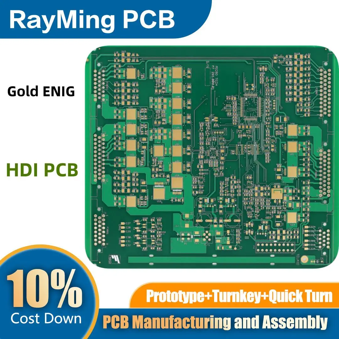
Gold ENIG 8 Layer HDI PCB refers to a sophisticated printed circuit board design that combines several advanced manufacturing techniques:
-
8 Layer: This PCB consists of eight conductive copper layers, allowing for complex circuit designs and high component density.
-
HDI (High-Density Interconnect): This technology uses microvias (tiny laser-drilled holes) and fine lines to increase circuit density and improve signal performance.
-
ENIG (Electroless Nickel Immersion Gold): This surface finish involves plating exposed copper with a layer of nickel, then a thin layer of gold.
Key features and benefits include:
- Excellent signal integrity due to shorter signal paths
- Reduced board size and weight
- Improved thermal management
- Enhanced electrical performance
- Flat surface finish ideal for fine-pitch components
- Extended shelf life and good solderability
- Suitable for high-frequency applications
This type of PCB is commonly used in advanced electronics such as smartphones, tablets, high-performance computing, and aerospace applications where space is at a premium and high reliability is crucial. The combination of HDI technology with ENIG finish ensures both high performance and durability.