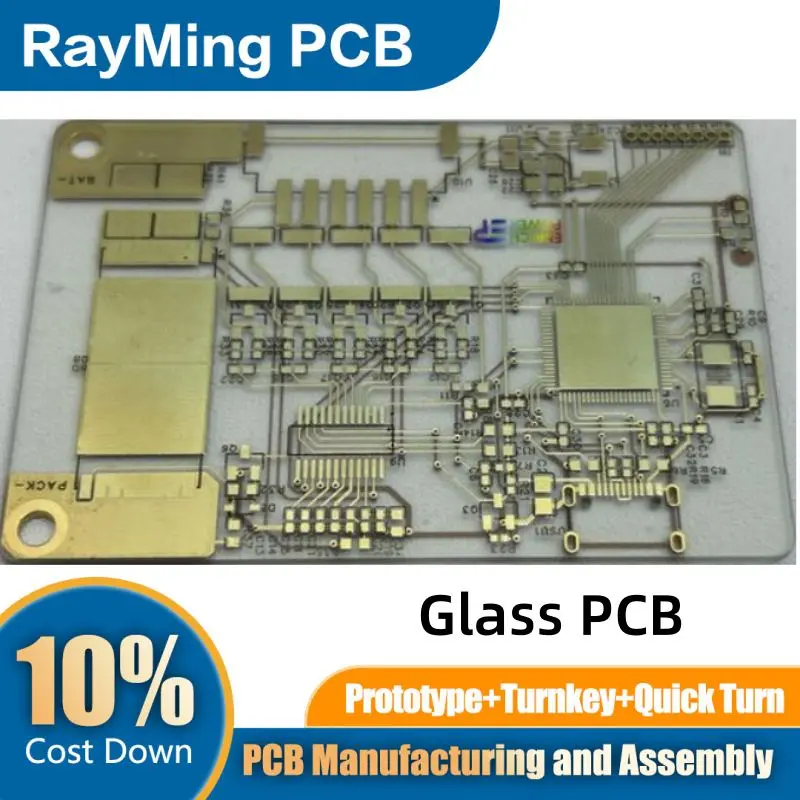
Glass printed circuit boards (PCBs) with thick gold plating represent a cutting-edge advancement in electronic substrate technology, combining the exceptional properties of glass substrates with the superior conductivity and reliability of thick gold metallization. This innovative approach addresses the growing demands of high-frequency, high-density, and high-reliability electronic applications where traditional organic substrates fall short.
Understanding Glass PCB Technology
Glass PCBs utilize ultra-thin glass sheets as the base substrate material instead of conventional fiberglass-reinforced epoxy resin (FR4). The glass substrate typically ranges from 30 to 200 micrometers in thickness, offering remarkable mechanical stability and dimensional precision. Unlike organic substrates that can experience thermal expansion, moisture absorption, and chemical degradation over time, glass provides an inert, stable platform that maintains its properties across extreme environmental conditions.
The manufacturing process involves creating conductive pathways through advanced techniques such as laser drilling for vias and photolithographic patterning for circuit traces. The glass surface undergoes specialized treatment to promote adhesion of subsequent metallic layers, creating a robust foundation for the thick gold plating process.
Thick Gold Plating: Beyond Standard Specifications
Traditional PCB gold plating typically ranges from 0.05 to 0.5 micrometers in thickness, primarily serving as a surface finish to prevent oxidation and ensure reliable connections. Thick gold plating, however, extends well beyond these conventional thicknesses, often reaching 2-10 micrometers or even thicker for specialized applications. This substantial gold layer transforms the electrical and mechanical characteristics of the circuit board.
The electroplating process for thick gold involves carefully controlled chemical baths containing gold salts, typically gold cyanide or gold sulfite solutions. The deposition rate, current density, temperature, and solution chemistry must be precisely managed to achieve uniform thickness distribution and optimal grain structure. Multiple plating cycles may be employed to build up the desired thickness while maintaining excellent adhesion and minimal internal stress.
Superior Electrical Performance
The combination of glass substrate and thick gold plating delivers exceptional high-frequency performance. Glass exhibits extremely low dielectric constant (typically 4-6) and virtually zero dielectric loss tangent across a wide frequency range, making it ideal for applications operating at millimeter-wave frequencies. The thick gold conductors provide minimal resistive losses and excellent current-carrying capacity, crucial for power electronics and high-speed digital circuits.
Signal integrity benefits significantly from this technology. The smooth glass surface and precise dimensional control minimize surface roughness effects that can cause signal attenuation at high frequencies. The thick gold plating reduces skin effect losses and maintains consistent impedance characteristics across the entire frequency spectrum, enabling reliable performance in 5G communications, automotive radar systems, and aerospace applications.
Thermal Management Advantages
Glass PCBs with thick gold plating excel in thermal management applications. While glass has relatively low thermal conductivity compared to ceramics, the thick gold layers create efficient heat conduction paths. Gold’s exceptional thermal conductivity (approximately 318 W/m·K) allows rapid heat dissipation from active components to thermal management systems.
The low coefficient of thermal expansion (CTE) of glass closely matches that of semiconductor devices, reducing thermal stress during temperature cycling. This CTE matching is particularly important for flip-chip and bare die attachment applications where thermal mismatch can lead to solder joint fatigue and connection failures.
Manufacturing Challenges and Solutions
Producing glass PCBs with thick gold plating presents unique manufacturing challenges. Glass processing requires specialized handling equipment and clean room environments to prevent contamination and breakage. The drilling of vias in glass substrates demands precise laser systems capable of creating clean, debris-free holes without inducing microcracks.
Thick gold plating introduces challenges related to stress management and adhesion. As gold thickness increases, internal stresses can develop that may cause delamination or warpage. Advanced plating chemistry and process control help mitigate these issues through stress-reducing additives and optimized deposition parameters. Surface preparation becomes critical, often involving multiple cleaning steps, chemical etching, and application of adhesion-promoting layers.
Quality control for thick gold plating requires sophisticated measurement techniques. X-ray fluorescence spectroscopy, cross-sectional microscopy, and electrical testing ensure uniform thickness distribution and proper adhesion. The high cost of gold necessitates precise process control to minimize waste while achieving target specifications.
Applications and Market Drivers
The primary applications for glass PCBs with thick gold plating span high-performance sectors where reliability and performance justify the premium cost. Telecommunications infrastructure, particularly 5G base stations and millimeter-wave antenna arrays, benefit from the superior RF performance. The automotive industry increasingly adopts this technology for advanced driver assistance systems (ADAS) and autonomous vehicle sensors operating at 77-81 GHz frequencies.
Aerospace and defense applications leverage the technology’s reliability in harsh environments. Satellite communications, radar systems, and electronic warfare equipment require the dimensional stability and corrosion resistance that glass substrates with thick gold plating provide. Medical device applications, particularly implantable electronics, benefit from the biocompatibility and long-term stability of gold surfaces.
Economic Considerations and Future Outlook
The cost of glass PCBs with thick gold plating significantly exceeds conventional alternatives, driven by expensive raw materials, specialized processing equipment, and lower manufacturing volumes. However, the total cost of ownership often favors this technology when factoring in improved reliability, reduced field failures, and enhanced performance capabilities.
Market trends indicate growing adoption as manufacturing processes mature and economies of scale develop. Advanced packaging technologies, including system-in-package (SiP) and heterogeneous integration, increasingly require the superior properties that glass substrates provide. The push toward higher frequency communications, autonomous vehicles, and Internet of Things (IoT) devices continues driving demand for this premium technology.
Conclusion
Glass PCBs with thick gold plating represent a convergence of advanced materials science and precision manufacturing techniques. While the technology commands premium pricing, its superior electrical performance, thermal management capabilities, and long-term reliability make it indispensable for next-generation electronic systems. As manufacturing processes continue to evolve and application demands increase, this technology will likely become more accessible while maintaining its position at the forefront of high-performance electronics. The combination of glass substrates and thick gold metallization offers a pathway to meeting the increasingly stringent requirements of modern electronic devices operating in demanding environments.