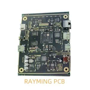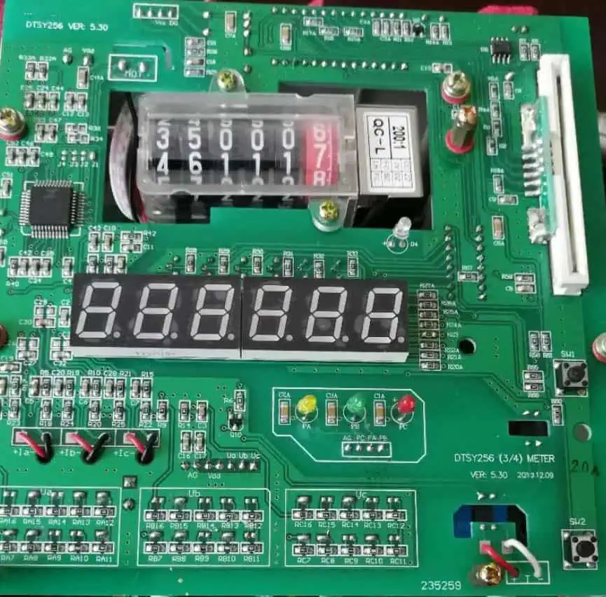
Energy meters are crucial components in modern power systems, allowing for accurate measurement and billing of electrical energy consumption. The heart of these devices lies in their Printed Circuit Boards (PCBs), which require careful design and manufacturing processes to ensure accuracy, reliability, and longevity.
PCB Design for Energy Meters
1. Component Selection
The first step in designing an energy meter PCB is selecting the appropriate components. Key components include:
- Microcontroller: Acts as the brain of the meter, processing data and controlling operations.
- Analog-to-Digital Converter (ADC): Converts analog signals from current and voltage sensors into digital data.
- Current and Voltage Sensors: Measure the electrical parameters of the power line.
- Real-Time Clock (RTC): Keeps track of time for accurate billing periods.
- Memory: Stores consumption data and meter configurations.
- Communication Modules: Enable remote reading and control (e.g., Wi-Fi, GSM, or Power Line Communication).
- Display: Shows consumption data and meter status to users.
2. Circuit Design
The circuit design phase involves creating schematics that define how all components interconnect. Key considerations include:
- Power Supply: Designing stable power rails for all components.
- Signal Integrity: Ensuring accurate measurement of low-level analog signals.
- EMI/EMC Compliance: Incorporating design elements to minimize electromagnetic interference.
- Calibration Circuitry: Including provisions for meter calibration during manufacturing.
3. PCB Layout
The PCB layout translates the schematic into a physical board design. Critical aspects include:
- Component Placement: Optimizing the placement for signal integrity and thermal management.
- Trace Routing: Designing traces to minimize noise and ensure signal quality.
- Ground Plane Design: Implementing a solid ground plane for noise reduction.
- Isolation: Separating high-voltage, low-voltage, and communication sections of the board.
- Thermal Management: Considering heat dissipation for power components.
4. Design for Manufacturing (DFM)
DFM ensures that the PCB can be efficiently and reliably manufactured. This includes:
- Adhering to manufacturing guidelines for trace widths, spacing, and drill sizes.
- Including fiducial marks for automated assembly.
- Designing test points for in-circuit testing.
PCB Manufacturing Process
1. PCB Fabrication
The PCB fabrication process involves several steps:
a) Imaging: The PCB design is transferred to the copper-clad board using photolithography.
b) Etching: Unwanted copper is removed, leaving only the desired circuit traces.
c) Drilling: Holes are drilled for through-hole components and vias.
d) Plating: Holes are plated with copper to create electrical connections between layers.
e) Solder Mask Application: A protective layer is applied to prevent solder bridges.
f) Silkscreen Printing: Component designators and other markings are printed on the board.
2. Component Assembly
Assembly of the PCB involves:
a) Solder Paste Application: Solder paste is applied to the PCB using a stencil.
b) Component Placement: Surface-mount components are placed using automated pick-and-place machines.
c) Reflow Soldering: The PCB is heated to melt the solder paste and secure the components.
d) Through-Hole Assembly: Manual or automated insertion of through-hole components.
e) Wave Soldering: For boards with through-hole components.
3. Testing and Quality Control
Rigorous testing is crucial for energy meter PCBs:
a) Automated Optical Inspection (AOI): Checks for missing components, incorrect placements, and solder defects.
b) In-Circuit Testing (ICT): Verifies electrical connections and basic component functionality.
c) Functional Testing: Tests the PCB’s ability to measure energy accurately under various conditions.
d) Calibration: Fine-tuning of the meter to ensure measurement accuracy.
e) Environmental Testing: Subjects the PCB to temperature cycles, humidity, and vibration to ensure durability.
4. Conformal Coating
Many energy meter PCBs receive a conformal coating to protect against moisture, dust, and chemical contaminants, enhancing long-term reliability.
Challenges and Considerations
Designing and manufacturing energy meter PCBs presents several challenges:
- Accuracy: Ensuring precise measurements over a wide range of current and voltage conditions.
- EMC Compliance: Meeting stringent electromagnetic compatibility standards for grid-connected devices.
- Long-Term Reliability: Designing for a operational life of 10-20 years under varying environmental conditions.
- Cost Optimization: Balancing performance requirements with cost constraints for mass production.
- Security: Implementing features to prevent tampering and unauthorized access to meter data.
- Regulatory Compliance: Meeting regional and international standards for energy metering devices.
Conclusion
The design and manufacturing of energy meter PCBs is a complex process that requires expertise in electrical engineering, manufacturing processes, and regulatory compliance. As smart grid technologies advance, energy meter PCBs are evolving to incorporate more features, such as power quality analysis, demand response capabilities, and integration with home energy management systems. This ongoing evolution ensures that energy meter PCB design and manufacturing will remain a critical and dynamic field in the power industry.