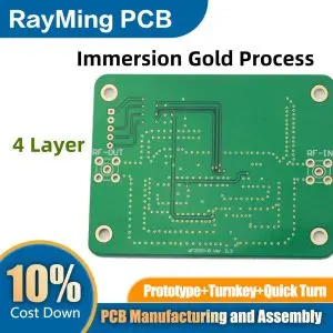
When designing complex electronic circuits, engineers often need more than the basic two-layer PCB configuration. An Altium 4 layer board provides the perfect balance between functionality, cost, and design complexity for intermediate to advanced electronic projects. This comprehensive guide will walk you through everything you need to know about designing 4-layer PCBs using Altium Designer.
What is an Altium 4 Layer Board?
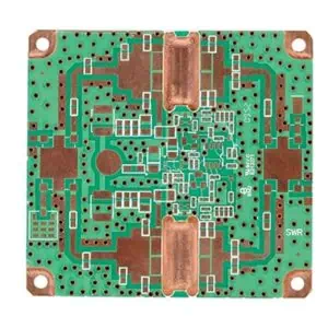
An Altium 4 layer board is a printed circuit board designed using Altium Designer software that consists of four conductive copper layers separated by insulating dielectric material. This multilayer configuration typically includes two signal layers (top and bottom) and two dedicated power/ground planes (inner layers), offering significant advantages over traditional 2-layer designs.
The standard 4-layer stackup arrangement places the power plane on layer 2 and the ground plane on layer 3, with signal routing on the top and bottom layers. This configuration provides excellent signal integrity, reduced electromagnetic interference (EMI), and improved power distribution throughout the circuit.
Why Choose a 4 Layer PCB Design?
Enhanced Signal Integrity
The primary advantage of an Altium 4 layer board lies in its superior signal integrity characteristics. The dedicated ground and power planes create a controlled impedance environment, reducing signal reflection and crosstalk between traces. This makes 4-layer designs essential for high-frequency applications, digital circuits operating above 10 MHz, and sensitive analog circuits.
Improved Power Distribution
With dedicated power and ground planes, your Altium 4 layer board ensures stable power delivery across the entire circuit. The large copper areas reduce power supply noise, provide low-impedance power paths, and create natural decoupling capacitance between the power and ground planes.
Better EMI Performance
The internal power and ground planes act as natural shields, significantly reducing electromagnetic emissions and improving the board’s immunity to external interference. This makes 4-layer designs ideal for products that must meet strict EMC compliance requirements.
Increased Routing Density
Four layers provide more routing space, allowing for more complex circuit designs while maintaining shorter trace lengths. This is particularly beneficial for dense digital circuits, microcontroller-based systems, and mixed-signal applications.
Altium Designer: The Professional Choice
Altium Designer stands out as the industry-leading PCB design software for creating professional 4-layer boards. Its comprehensive toolset includes advanced routing capabilities, built-in design rule checking (DRC), and sophisticated layer stack management features that streamline the 4-layer design process.
Key Altium Features for 4 Layer Design
Layer Stack Manager: Altium’s Layer Stack Manager allows precise control over your 4-layer stackup, including dielectric thickness, copper weights, and impedance calculations. This ensures your design meets manufacturing specifications and performance requirements.
Interactive Routing: The software’s push-and-shove routing technology makes it easy to navigate traces around components while maintaining design rules, particularly important in the constrained space of a 4-layer design.
3D Visualization: Altium’s 3D rendering capabilities let you visualize your 4-layer board design before manufacturing, helping identify potential mechanical conflicts and assembly issues.
Designing Your First Altium 4 Layer Board
Step 1: Project Setup and Stack Definition
Begin by creating a new PCB project in Altium Designer. Access the Layer Stack Manager to define your 4-layer configuration. The typical stackup includes:
- Layer 1: Top Signal Layer
- Layer 2: Power Plane (VCC)
- Layer 3: Ground Plane (GND)
- Layer 4: Bottom Signal Layer
Configure the dielectric thickness between layers (typically 0.1-0.2mm for standard designs) and specify copper weights for each layer.
Step 2: Component Placement Strategy
Proper component placement is crucial for 4-layer board success. Place critical components first, considering signal flow and power requirements. Position high-speed digital components near the center of the board to minimize trace lengths and take advantage of the internal plane shielding.
Step 3: Power and Ground Plane Design
Design your power and ground planes with careful attention to plane splits if multiple power domains are required. Use thermal reliefs for through-hole components to prevent soldering difficulties while maintaining electrical connectivity.
Step 4: Signal Routing Optimization
Route critical signals first, using the top and bottom layers primarily for signal traces. Minimize layer changes (vias) for high-speed signals, and maintain consistent trace impedance by following your calculated design rules.
Best Practices for Altium 4 Layer Boards
Via Management
Strategic via placement is essential in 4-layer designs. Use buried vias sparingly as they increase manufacturing costs. Standard through-hole vias connecting all four layers are more cost-effective and provide reliable connections.
Thermal Considerations
Plan for adequate thermal management by incorporating thermal vias to transfer heat from surface-mount components to internal planes. This is particularly important for power semiconductors and high-current applications.
Design Rule Configuration
Configure Altium’s design rules carefully to reflect your manufacturing capabilities and electrical requirements. Set appropriate trace widths, via sizes, and spacing rules to ensure manufacturability while meeting performance specifications.
Manufacturing Considerations
When preparing your Altium 4 layer board for manufacturing, generate comprehensive fabrication outputs including Gerber files, drill files, and assembly drawings. Clearly specify the stackup requirements, including dielectric materials and copper weights, in your fabrication notes.
Most PCB manufacturers can easily produce 4-layer boards using standard FR4 materials and processes, making them cost-effective for medium to high-volume production. Expect manufacturing costs approximately 2-3 times higher than equivalent 2-layer designs.
Common Applications
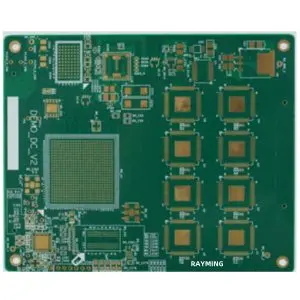
Altium 4 layer boards excel in various applications including microcontroller-based systems, communication devices, automotive electronics, industrial control systems, and consumer electronics requiring EMC compliance. They’re particularly valuable for designs incorporating mixed-signal circuits, high-speed digital interfaces, or multiple power domains.
Conclusion
Mastering the Altium 4 layer board design process opens doors to more sophisticated electronic product development. The combination of Altium Designer’s powerful tools and the enhanced capabilities of 4-layer construction provides the foundation for professional, reliable electronic designs that meet modern performance and compliance requirements.
Whether you’re developing your first 4-layer design or looking to optimize existing projects, understanding these principles and best practices will help you create successful products that leverage the full potential of multilayer PCB technology.