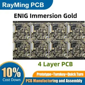
The Electroless Nickel Immersion Gold (ENIG) plating process for 4-layer PCBs involves several critical steps:
-
Cleaning: The PCB is thoroughly cleaned to remove contaminants, ensuring optimal adhesion.
-
Micro-etching: A mild etching process roughens the copper surface, improving nickel adhesion.
-
Catalyzation: A palladium catalyst is applied to initiate the electroless nickel deposition.
-
Electroless Nickel Plating: Nickel is deposited without electricity, forming a 3-6 µm layer. This step is crucial for 4-layer PCBs, providing a uniform coating across complex topographies.
-
Immersion Gold Plating: A thin gold layer (0.05-0.1 µm) is deposited through ion exchange, displacing surface nickel atoms.
-
Rinsing and Drying: The PCB is thoroughly rinsed and dried to remove residual chemicals.
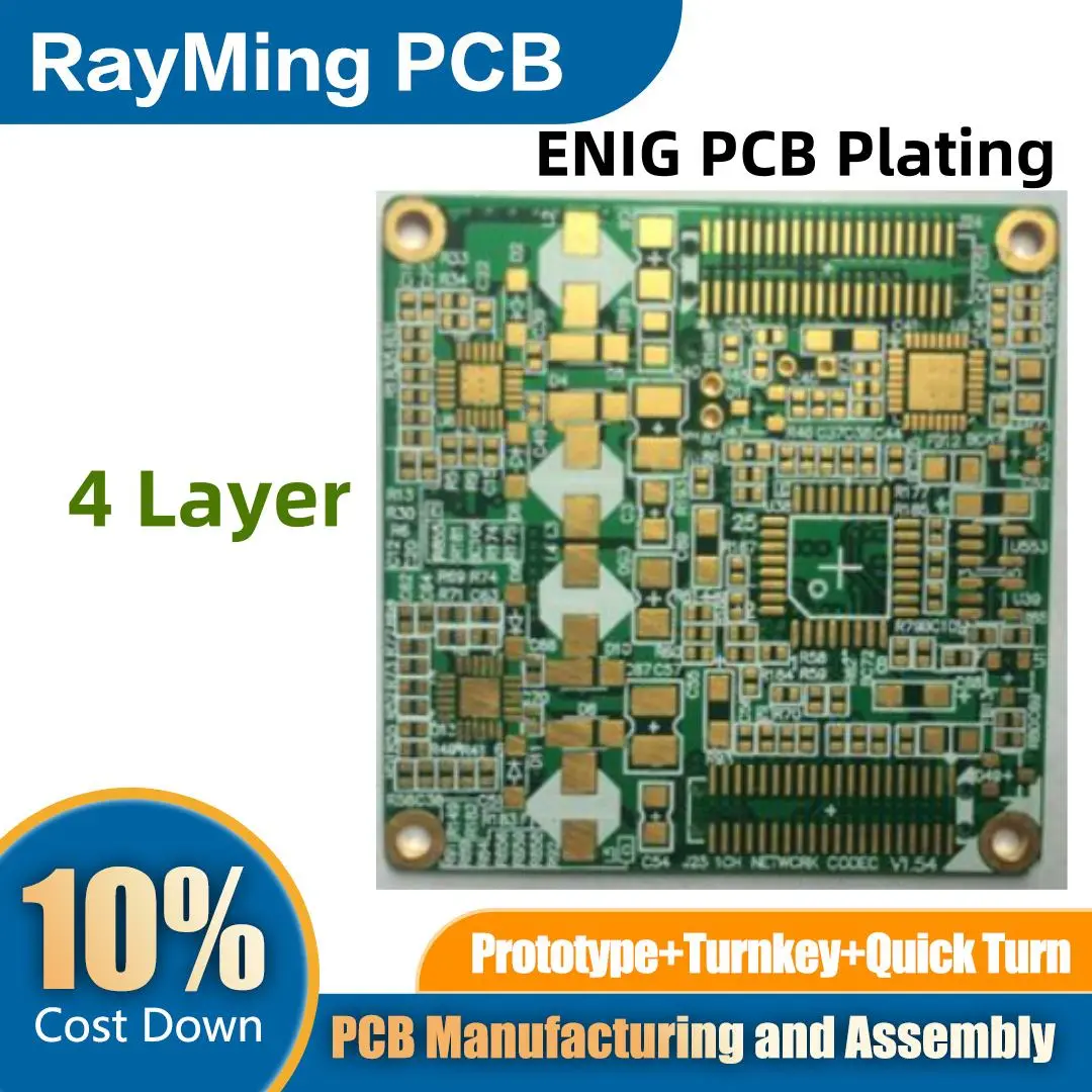
In 4-layer PCBs, ENIG plating offers several advantages:
- Excellent planarity for dense, fine-pitch components
- Uniform thickness across all layers, crucial for impedance control
- Enhanced corrosion resistance for longer shelf life
- Compatibility with both leaded and lead-free soldering processes
The ENIG plating process, while more complex than some alternatives, provides superior performance and reliability for sophisticated 4-layer PCB designs used in high-end electronics.