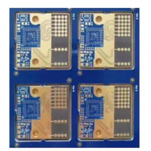
Product Overview
Our Advanced Packaging PCB IC Package Substrate represents the cutting edge of semiconductor packaging technology, designed to meet the demanding requirements of high-performance integrated circuits in today’s most sophisticated electronic applications.
Key Features
Ultra-High Density Interconnect (HDI) Technology Features fine-pitch via structures and multiple buildup layers enabling exceptional routing density for complex multi-die packages and system-in-package (SiP) applications.
Superior Electrical Performance Engineered with low-loss dielectric materials and controlled impedance design to minimize signal degradation, reduce crosstalk, and maintain signal integrity at high frequencies up to millimeter-wave applications.
Advanced Thermal Management Incorporates embedded thermal vias, copper coin technology, and optimized layer stackup to efficiently dissipate heat from high-power semiconductor devices, ensuring reliable operation under demanding thermal conditions.
Precision Manufacturing Manufactured using state-of-the-art processes with tolerances as tight as ±25μm for critical dimensions, ensuring consistent quality and yield for advanced packaging applications.
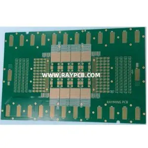
Technical Specifications
- Layer Count: 4-20+ layers with microvias
- Minimum Via Size: 50μm diameter
- Line Width/Spacing: Down to 15/15μm
- Dielectric Materials: Low-Dk/Df materials optimized for high-frequency performance
- Surface Finish: Multiple options including ENIG, OSP, and immersion silver
- Package Types: BGA, QFN, CSP, FC-BGA, and custom configurations
Applications
Ideal for advanced semiconductor packaging in telecommunications infrastructure, data center processors, automotive electronics, AI/ML accelerators, 5G/6G wireless systems, and high-performance computing applications where miniaturization, performance, and reliability are critical.
Quality & Reliability
Manufactured in ISO 9001:2015 certified facilities with comprehensive testing including electrical continuity, impedance verification, thermal cycling, and reliability stress testing to ensure consistent performance in mission-critical applications.
Our Advanced Packaging PCB substrates enable semiconductor manufacturers to push the boundaries of integration density and performance while maintaining the highest standards of quality and reliability.