When developing complex electronic products, a 4 layer PCB prototype often becomes essential for achieving optimal performance and reliability. This comprehensive guide explores everything you need to know about 4-layer printed circuit board prototypes, from design considerations to manufacturing processes.
What is a 4 Layer PCB Prototype?
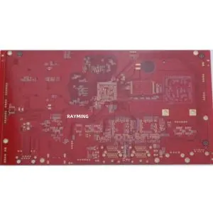
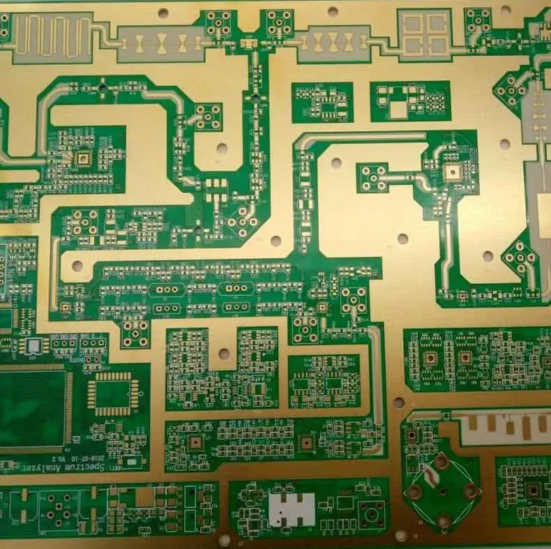
A 4 layer PCB prototype is a printed circuit board consisting of four conductive copper layers separated by insulating dielectric materials. Unlike single or double-layer boards, this configuration provides enhanced functionality through dedicated power and ground planes, improved signal integrity, and better electromagnetic interference (EMI) shielding.
The typical 4-layer stackup includes:
- Top layer: Component placement and signal routing
- Ground plane: Provides electrical reference and EMI shielding
- Power plane: Distributes power throughout the circuit
- Bottom layer: Additional signal routing and component placement
Why Choose a 4 Layer PCB Prototype?
Enhanced Signal Integrity
4 layer PCB prototypes offer superior signal integrity compared to simpler designs. The dedicated ground and power planes create controlled impedance environments, reducing signal reflections and crosstalk between traces. This becomes crucial when working with high-frequency signals or sensitive analog circuits.
Improved Power Distribution
With a dedicated power plane, your 4 layer PCB prototype ensures stable voltage distribution across all components. This reduces voltage drops, minimizes power-related noise, and improves overall circuit performance. The power plane acts as a low-impedance path for current flow, essential for power-hungry components.
Better EMI Performance
The ground plane in a 4 layer PCB prototype serves as an effective EMI shield, containing electromagnetic emissions within the board while protecting sensitive circuits from external interference. This is particularly important for products that must meet regulatory compliance standards.
Space Optimization
Despite having four layers, a well-designed 4 layer PCB prototype can be more compact than equivalent 2-layer designs. The additional routing layers allow for more efficient trace placement, reducing the overall board size while maintaining functionality.
Design Considerations for 4 Layer PCB Prototypes
Layer Stack-up Planning
Proper layer stack-up is critical for 4 layer PCB prototype success. The most common configuration places the power and ground planes in the middle layers, with signal layers on the top and bottom. This arrangement provides excellent shielding and power distribution while allowing flexible component placement.
Via Design and Placement
Vias connect different layers in your 4 layer PCB prototype, but they also consume valuable real estate and can affect impedance. Minimize via usage where possible, and consider using blind or buried vias for high-density designs. Proper via placement ensures reliable interlayer connections without compromising signal integrity.
Component Placement Strategy
Strategic component placement on your 4 layer PCB prototype maximizes performance and manufacturability. Place high-frequency components close to their associated circuits, keep analog and digital sections separated, and ensure adequate spacing for thermal management. Consider the manufacturing process when placing components to avoid assembly issues.
Power and Ground Plane Design
Effective power and ground plane design is crucial for 4 layer PCB prototype performance. Avoid splitting planes unnecessarily, as this can create return path issues. Use adequate copper pour for current-carrying capacity, and implement proper decoupling capacitor placement to minimize power supply noise.
Manufacturing Process for 4 Layer PCB Prototypes
Material Selection
Choose appropriate materials for your 4 layer PCB prototype based on application requirements. Standard FR-4 works well for most applications, while high-frequency designs may require specialized low-loss materials. Consider factors like dielectric constant, loss tangent, and thermal properties when selecting materials.
Fabrication Steps
The manufacturing process for 4 layer PCB prototypes involves several critical steps:
Substrate Preparation: Individual layers are prepared with copper cladding and cleaned for processing.
Layer Processing: Each layer undergoes photolithography to define circuit patterns, followed by etching to remove unwanted copper.
Lamination: The four layers are stacked with prepreg (pre-impregnated fiberglass) between them and laminated under heat and pressure.
Drilling: Holes for vias and component mounting are drilled using precision equipment.
Plating: Holes are plated to create electrical connections between layers.
Surface Finishing: The final surface finish is applied to protect copper and ensure good solderability.
Quality Control
Rigorous quality control ensures your 4 layer PCB prototype meets specifications. This includes electrical testing to verify connectivity and isolation, dimensional inspection to confirm mechanical accuracy, and visual inspection to identify defects. Advanced testing may include impedance measurement and thermal cycling.
Applications for 4 Layer PCB Prototypes
Consumer Electronics
4 layer PCB prototypes are common in smartphones, tablets, and other compact consumer devices where space is limited but performance requirements are high. The multilayer design enables complex functionality in minimal space.
Industrial Controls
Industrial control systems benefit from the noise immunity and power distribution capabilities of 4 layer PCB prototypes. These applications often require reliable operation in harsh environments with significant electromagnetic interference.
Medical Devices
Medical electronics frequently use 4 layer PCB prototypes to achieve the reliability and performance required for critical applications. The enhanced signal integrity helps ensure accurate sensor readings and reliable device operation.
Automotive Electronics
Modern vehicles contain numerous electronic systems that rely on 4 layer PCB prototypes for reliable operation. These boards must withstand temperature extremes, vibration, and electromagnetic interference common in automotive environments.
Tips for Successful 4 Layer PCB Prototype Development
Work with Experienced Manufacturers
Partner with PCB manufacturers who have proven experience with 4 layer designs. They can provide valuable design feedback and ensure your prototype meets manufacturing requirements.
Plan for Testing
Design test points and debug features into your 4 layer PCB prototype from the beginning. This facilitates troubleshooting and validation during the development process.
Consider Assembly Requirements
Think about component assembly during the design phase. Ensure adequate spacing for pick-and-place equipment, consider component orientation for automated assembly, and plan for inspection access.
Optimize for Cost
While 4 layer PCB prototypes cost more than simpler designs, smart design choices can minimize expense. Standardize via sizes, avoid unnecessary complexity, and design for standard manufacturing processes.
Conclusion
A well-designed 4 layer PCB prototype provides the foundation for successful electronic product development. By understanding the design principles, manufacturing processes, and application considerations outlined in this guide, you can create prototypes that meet your performance requirements while remaining manufacturable and cost-effective.
Whether you’re developing consumer electronics, industrial controls, or specialized applications, the enhanced capabilities of 4 layer PCB prototypes make them an excellent choice for complex electronic designs. Work with experienced design teams and manufacturers to ensure your prototype development process runs smoothly and produces reliable results.