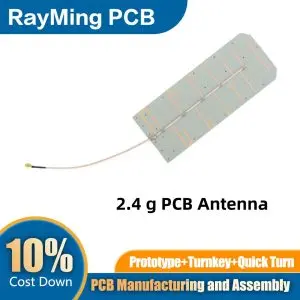
The 2.4 GHz embedded PCB antenna has become a fundamental component in modern wireless communication systems, particularly for Wi-Fi receivers. These compact, cost-effective antennas are integrated directly into the printed circuit board (PCB) of electronic devices, eliminating the need for external antennas and reducing both manufacturing costs and device footprint.
Design Fundamentals
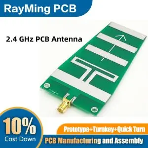
Embedded PCB antennas for 2.4 GHz Wi-Fi applications are typically designed as microstrip patch antennas, inverted-F antennas (IFA), or planar inverted-F antennas (PIFA). Each design has specific characteristics that make it suitable for different applications:
Microstrip patch antennas consist of a metal patch on one side of a dielectric substrate with a ground plane on the opposite side. They provide good directional radiation patterns and moderate bandwidth but require more PCB real estate.
Inverted-F antennas feature an “F” shaped conductor with one end connected to the ground plane and the other end open. These antennas offer good omnidirectional coverage while maintaining a compact form factor.
PIFAs are similar to IFAs but incorporate a planar element parallel to the ground plane, improving bandwidth and efficiency in a relatively small footprint. This design is particularly popular in mobile devices.
Critical Design Parameters
Several parameters significantly influence the performance of 2.4 GHz PCB antennas:
Substrate Material: The dielectric constant (εr) and loss tangent of the PCB substrate directly affect antenna efficiency and bandwidth. FR-4, with εr ≈ 4.4, is commonly used due to its low cost, though materials like Rogers RO4350B offer superior RF performance for high-end applications.
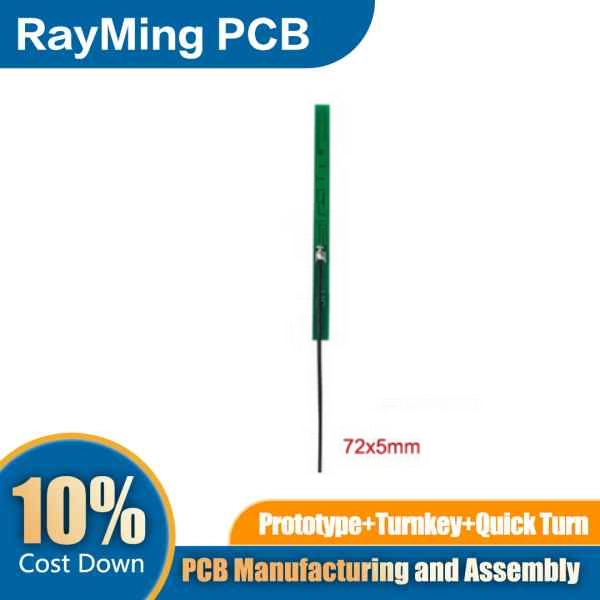
Antenna Dimensions: The physical dimensions of the antenna element must be carefully calculated based on the operating wavelength and substrate properties. For 2.4 GHz (wavelength ≈ 125 mm), typical PCB antenna elements range from 10-30 mm depending on the design.
Ground Plane Size: The ground plane significantly influences antenna impedance and radiation pattern. Inadequate ground plane dimensions can cause performance degradation, especially in compact devices.
Matching Network: Most embedded antennas require an impedance matching network to optimize power transfer between the transceiver and antenna. This typically consists of capacitors and inductors arranged in configurations like pi or T networks.
Manufacturing Considerations
Fabricating effective 2.4 GHz PCB antennas requires attention to several manufacturing aspects:
Trace Width and Spacing: Precise control of trace dimensions is crucial for maintaining the antenna’s designed impedance characteristics. Industry standard PCB manufacturing processes typically allow for trace widths down to 0.1 mm with tolerances of ±10%.
Layer Stackup: The thickness and arrangement of PCB layers affect antenna performance. Designers must consider the distance between the antenna element and ground plane, which influences bandwidth and efficiency.
Soldermask and Silkscreen: These layers can alter the effective dielectric constant around the antenna. In high-performance designs, soldermask is often removed from the antenna area to maintain consistent electrical properties.
Surface Finish: The conductivity of the antenna element is affected by the PCB’s surface finish. ENIG (Electroless Nickel Immersion Gold) provides good conductivity and oxidation resistance for RF applications.
Performance Metrics
Several key metrics define the performance of 2.4 GHz PCB antennas:
Return Loss/VSWR: Return loss (typically expressed in dB) indicates how well the antenna is matched to the transmission line. A return loss greater than 10 dB (equivalent to VSWR < 2) is generally acceptable for Wi-Fi applications.
Radiation Pattern: The spatial distribution of radiated energy affects coverage. Omnidirectional patterns are preferred for most Wi-Fi applications, though directional patterns may be advantageous in specific use cases.
Gain: Typically ranging from 2-5 dBi for PCB Wi-Fi antennas, gain represents the antenna’s ability to direct energy in a specific direction compared to an isotropic radiator.
Efficiency: This metric indicates what percentage of input power is actually radiated, with well-designed PCB antennas achieving 70-90% efficiency depending on substrate quality and design optimization.
Bandwidth: The 2.4 GHz Wi-Fi band spans 2.4-2.485 GHz, requiring antennas to maintain acceptable performance across this frequency range.
Integration Challenges
Integrating 2.4 GHz PCB antennas into complete systems presents several challenges:
Proximity Effects: Nearby components, especially metallic parts like shields or batteries, can detune the antenna by capacitive coupling or blocking radiation paths. Maintaining adequate clearance zones around the antenna is essential.
Housing Influence: Device enclosures, particularly those containing metal or high-dielectric materials, can significantly alter antenna performance. Simulation and testing with the actual housing are crucial steps in the design process.
EMI Considerations: The antenna can both receive and generate electromagnetic interference. Proper isolation from sensitive circuits and attention to EMI regulatory requirements are necessary.
Multi-antenna Systems: Modern devices often incorporate multiple antennas for MIMO (Multiple-Input Multiple-Output) operation. Antenna placement must consider isolation between elements to minimize mutual coupling.
Applications
Embedded PCB antennas for 2.4 GHz Wi-Fi reception find applications across numerous devices:
IoT Devices: Smart home sensors, thermostats, and monitoring systems benefit from the compact, low-cost nature of PCB antennas.
Consumer Electronics: Laptops, tablets, and smart TVs incorporate embedded antennas to maintain aesthetic design while providing reliable connectivity.
Industrial Equipment: Factory automation systems and industrial IoT devices utilize PCB antennas for wireless monitoring and control networks.
Medical Devices: Patient monitoring systems and portable diagnostic equipment leverage these antennas for reliable wireless data transmission.
Wearable Technology: Fitness trackers, smartwatches, and health monitors benefit from the small footprint and power efficiency of well-designed PCB antennas.
Future Trends
The evolution of 2.4 GHz PCB antenna technology continues along several trajectories:
Miniaturization: As devices become smaller, antenna designs that maintain performance while reducing size are increasingly valuable.
Multi-band Operation: Antennas capable of operating efficiently in both 2.4 GHz and 5 GHz bands from a single element address the growing demand for dual-band Wi-Fi connectivity.
Integration with Other Components: Antennas that double as structural elements or incorporate additional functionality (like NFC coils) maximize space utilization in compact devices.
Advanced Materials: Metamaterials and engineered substrates offer potential for improved efficiency and bandwidth in reduced footprints.
Adaptive Designs: Electronically tunable antennas that can adjust their characteristics based on operating environment or user conditions represent the cutting edge of antenna development.
The humble 2.4 GHz embedded PCB antenna remains a critical component in our increasingly wireless world. Through careful design, simulation, and testing, these inconspicuous elements enable the connectivity we depend on daily, balancing performance requirements with practical manufacturing and integration constraints. As wireless technology continues to evolve, so too will the designs and capabilities of these essential components, expanding the possibilities for connected devices across all aspects of modern life.