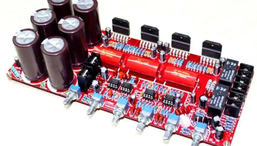
One of the most popular audio chip amplifier is the LM3886. It is well-established in DIY markets. It is compelling for use for a variety of reasons. There are fewer equivalents and less distortion, which makes it more affordable.
In order for all of these components to work together to create a great audio amplifier which is unequaled as regards performance and cost, it is crucial to choose the right arrangement and equivalents for such chips.
Considerations Before Creating the Lm3886 PCB
When creating audio amplifiers, there are a few important factors to consider. Output power is the major element.
Before the setup of the full chip production process, it must be decided. An amplifier board’s typical output falls between 60 and 68 watts. However, depending on the desired outcome, this may change. Voltage and Impedance are two more considerations. The impedance of various speakers varies.
For convenience, it’s continually accessible in your user manual. Moreover, a particular input voltage is required for the whole manufacturing. The audio chip amplifiers will base its work on this factor in order to amplify the output. These parameters are all set and analyzed by various mobile applications.
With the use of a specialized instrument called the multimeter, it is preferable to work in accordance with AC voltage seen between various channels of such an audio chip.
Calculating the Power Needed for the Lm3886 PCB
Setting the power and voltage of the power supply is the subsequent step. Again, these variables vary depending on the speaker type. They are also important in accurately determining the transformer’s VA score in audio chips.
This will produce the power required for its efficient operation. Transformers often have lower voltage, and since they are present, its amplifier’s output power will likewise be lower. If the transformer’s VA score is less than average, it will have a detrimental effect on audio chips by causing audio to be disrupted when this volume is increased by users.
Power Supply Voltage Audio Amplifier Lm3886 PCB
It is crucial to assess the amplifier’s peak output voltages while you are operating on it. Working upon this power supply voltages is the next phase.
Designing the Ground Layout for the Lm3886 PCB
The amplifier’s output is connected directly to the amplifier’s base layout that is being developed. A layout must be faultless in order to carry out its intended purposes. The amplifier would output nothing when the speakers are turned off, which is number one.
Even without any music playing, faulty ground layouts will cause them to emit a noticeable hum sound. The problems with the ground layouts can be fixed with the right guidelines. Less current should flow through the ground and more current must flow out of the ground and with a greater degree. Low current grounds can be connected to loops and the input circuitry.
Speakers, the Zobel network, and power supply capacitor all have grounds with high current. It matters how the stream travels from the high ground to the low current ground. It generates DC offset voltages as well as naturally amplifies the sound to improve it. There’s a practical way to maintain a safe spacing between areas with low as well as high current grounds. Now, let’s take some time to talk about them.
When the aforementioned grounds come into constant touch with the primary system ground, issues arise. This main ground will be placed nearer to capacitors present on the circuit for power supply that serve as reservoirs. The main ground’s purpose is to connect its earth wire to its amplifier chassis and to a unique circuit known as loop protection circuits.
Design Process of the Lm3886 PCB

The final act of the amplifier is determined by the PCB designs. We will go into more detail on how to create a precise printed circuit board layout. To create an amplifier, two circuits are required.
EasyEDA is one well known outstanding resources in this effort. In order to create such layouts and designs, a comprehensive package is required. These circuits’ schematics are available on the LM3886 PCB. The program is a completely free one that can also manage printed circuit board fabrication and production on a custom basis.
placing circuit board orders
In this unique PCB tool, a button named “Fabrication Output” can be found. It directs consumers to a different page where they can order their preferred circuit boards. Furthermore, t here are various alternatives accessible to choose from, including the copper’s thickness, the printed circuit board’s overall size, the circuit’s color, and the number of components (circuit boards).
Guidelines for the Lm3886 PCB Design
To make high-quality circuit boards and amplifiers, it is best to adhere to the instructions. The high current level that passes through and finds its way between these power supply voltages allows this magnetic field to form. This known magnetic field can be seen as crucial for creating a current inside its input traces as well as the loop.
For effective operation, there ought to be spacing in a right-angle between the two boards. This distance aids in the circuit’s efficient routing. Also aids in as much distortion reduction as possible. To make routing simpler, these should likewise be located on opposite sides of its terminals.
Any remaining space results in the development of an additional loop which receives incoming transmission and disrupts the generated electromagnetic field. In order to reduce the likelihood of creating another loop, those traces which are linked to the supply of power as well as power ground ought to be positioned and routed inside a very close periphery. Similarly, the audio input and signal traces function better when they get closer or are closer together.
It also lessens the possibility of creating any extra loop which might interrupt the entire process whenever ground planes get positioned on the PCB’s lower layer.
Only signal ground, as well as power ground, are predicated in the printed circuit board ground network. Each of the grounds has its own specific ground plane. This signal ground has low current as well as the power ground, which has a very high current.
More Guidelines
Until both grounds make contact with its major ground system, they are separated by a significant distance. The circuit board’s upper layer contains the power supply, Zobel network, and output. According to the rules, their routing is carried out on a ground plane.
Loops and circuit board input are included in signal ground planes. In order to manage the supply of power and reduce resistance and inductance across the whole circuitry, there must be a significant space between these traces.
This problem with inductive loads would be that, when used in conjunction with series capacitors, they resist smooth flow of current and cause resonance. Moreover, it lengthens the trace, however this is not necessary for this unique pursuit.
To prevent these issues, it’s critical to keep every one of these traces short. The same holds true for additional elements like loops, the Zobel network, as well as input. Placing all of these circuit components in opposition to the audio chip’s pins is one way to keep these traces short.
Wiring the Circuit Board Together
Humans make advantage of every component of audio chip amplifiers that is appropriate for this use. The entire cost of the product’s channel used ranges between $100 to $118. The amplifier wiring, chassis, and components for power supply are not included in the price.
The amplifier can be produced for a lot less money. To even further process items in a productive way, it is crucial to change these sections’ corresponding footprints in your design.
Lm3886 PCB Layout Using Soldering and Solder Paste
Before starting the soldering, there is a crucial step to do. Sandpaper can be used to remove oxidation before assembling the circuit parts. This step’s advantage is that it helps the process of soldering create a covert connection that improves electrical conductivity.
During the process of soldering, it is essential to arrange and transport the components of the circuit on the puffy cloth. On the circuit’s upper surface, everything takes place. Soldering all smaller circuit components first is crucial before the bigger ones.
Eutectic solder has far higher quality than typical tin-lead solder. More room for melting is provided.
When one or more of these circuit components move from their initial position, it also creates an additional cold solder joint. Using the solder has stronger electrical connectivity as well as quick setting as advantages.
Chassis Detection
The circuit components are kept safe and sound in a designated area to prevent damage to them throughout any process. To prevent interference from lights and radios, the wires as well as all connectors require a certain container-like construction. The search for a chassis which is appropriate for the kind of circuit is a challenge.
Conclusion
The LM3866 PCB is one of the most popular audio chip amplifier PCBs. It is well-established in DIY markets. It is compelling for use for a variety of reasons. Read through the article over again to understand better.