KiCad is a free, open source electronics design automation suite for Windows, Mac, and Linux, widely used by hobbyists, makers, and engineers to design printed circuit boards (PCBs).
Converting your KiCad schematic to PCB layout is an essential step in the process of designing a custom PCB, allowing you to define the physical board and component layout matching your circuit schematic connectivity.
This article provides a step-by-step workflow to successfully move from schematic capture to populated PCB layout using KiCad version 5.1.9’s schematic and PCB editor tools. Screenshots illustrate the key steps.
Let’s get started!

KiCad Design Flow Basics
Below are the basic work stages as you move from concept to finished PCB manufacturing file output when using the KiCad EDA tool suite:
- Schematic Capture – Draw circuit diagram connecting components with nets
- Schematic Symbols Creation – Make new parts with unique symbols and footprints
- Schematic Annotations – Assign reference designators to parts
- Netlist Generation – Output connectivity netlist file (.net)
- Footprint Assignment – Associate footprints to schematic parts
- Design Rule Check – Validate schematic for ERC/DRC errors
- PCB Layout – Convert netlist to board with parts placed and routed
- Gerber File Generation – Manufacturing output from PCB
We will focus specifically on steps 4 to 7 which enable progression from completed schematic diagram to functional PCB layout, ready for fabrication.
Generate Netlist File From Schematic
Once your schematic circuit drawing in the KiCad Eeschema schematic editor is logically complete with part symbols wired by nets representing connectivity just like the circuit should operate in physical reality, we are ready to move from schematic to board layout.
The NETLIST file acts as the bridge between the schematic sheet components connectivity and the layout board definition.
To generate a netlist:
- Select menu
Tools > Generate Netlist Files - Select the checkbox for format
Pcbnew (*.net) - Enter filename
test_boardfor the netlist - Select checkbox option
Generate single net for unconnected pins - Click
OKbutton
This will generate test_board.net file with net connectivity data matching your schematic diagram’s circuit logic.
The key output netlist formats from Eeschema used at different points in the PCB design process are:
| Netlist Format | Description |
|---|---|
| .net | PCBNew format used for PCB layout routing |
| .xml | PCBNew format used to import custom schematic footprints |
| .bom | Bill of Materials format for assembly |
For now, we need the .net PCBNew netlist file that has extracted nets and component connectivity intelligence from the schematic.
Time to move to the PCB Layout editor.
Import Netlist into PCBNew Layout Tool
The PCB Layout editor tool within KiCad is named Pcbnew. This is the canvas where we will map our schematic circuit’s logical connectivity defined graphically in Eeschema down onto the physical domain of the PCB board that will be manufactured.
To import the generated netlist file:
- Launch
Pcbnewfrom the KiCad toolbar - Go to menu
File > Import Netlist - A dialog prompts you to select the
*.netnetlist file previously created. - Select the checkbox option
Keep Existing Libraries - Click
OK
This will open up the main PCB layout canvas and import all the parts and nets defined in our source schematic, ready for board layout work.
Run Electrical Rules Check
Before rushing into board layout placement and routing, it is good practice to run an electrical rules check on the imported netlist to spot any violations with component pin mappings or missing connections compared to the schematic.
Go to top toolbar Tools > Electrical Rules Check
KiCad will analyze the entire netlist and schematic connectivity, flagging warnings if finds any:
- Unresolved component pin numbers conflicts when mapping schematic symbols to PCB footprints
- Missing connections / continuity issues versus the schematic sheet
- Duplicate reference designators assigned
- Etc.
Address any errors or warnings reported at this stage before further progressing the design conversion. Once ERC passes cleanly, we can be confident to continue with component placement and layout work confident that the PCB connectivity matches the schematic completely.
Assign PCB Footprints to Components
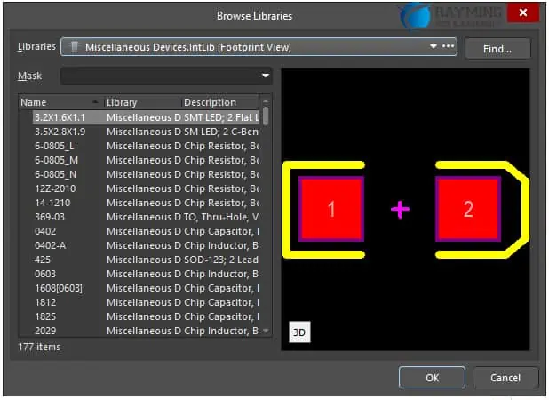
Every schematic symbol needs a matching PCB footprint assigned, which defines the physical land pattern on the board matching how component terminals will eventually solder down.
To assign footprints:
- With PCB board open, select menu
Tools > Assign Footprints - A spreadsheet loads with list of all schematic parts.
- Choose matching PCB footprint required from libraries already installed for each part.
- Saved selections automatically get mapped.
Repeat for all components ensuring every part has both:
- Unique schematic symbol in schematic editor
- Corresponding PCB footprint in Pcbnew layout tool
This cross-mapping connects the gates and pins of abstract schematic symbols to real solderable terminations on board.
PCB Layout Design Setup
Before placement and routing, some initial PCB layout design rule and workspace configurations need defining first:
- Board outline dimensions
- Copper layer counts
- Grid & Component clearance rules
- Net classes for trace widths/clearances
- Routing zones definition
- Layer stack table
Tools under Design Rules and Preferences menus allow correctly pre-setting these parameters matching circuit needs and capabilities of your PCB fabrication process.
For a simple single-sided PCB:
- Define rectangular board dimensions under Page Settings
- Add Keepout layer graphical boundary showing max size
- Set 50mil grid spacing under Preferences
- Define clearance rules between tracks, pads, vias
- Map layers to physical PCB fabrication layers
Default settings tables can be used initially and refined later once placement is underway.
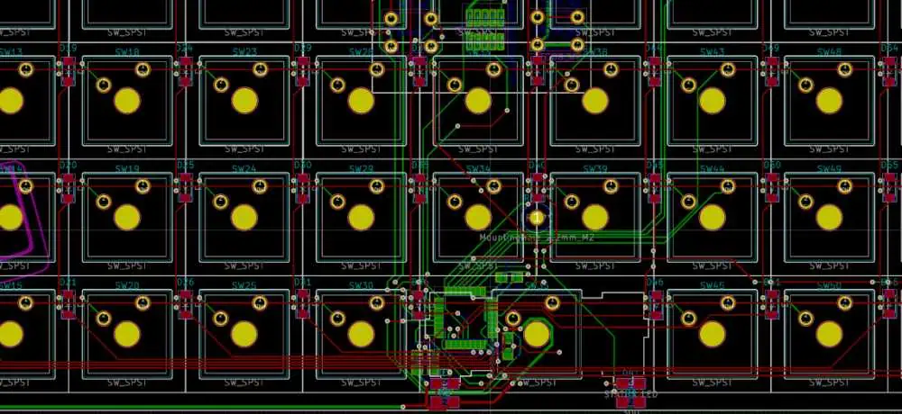
Begin Component Placement
We can now start intelligently placing components on the PCB canvas to gradually transform from rats nest to routed board layout matching schematic.
Steps for component placement:
- Select component to place from list of imported parts from schematic
- Move crosshair cursor to desired location on board
- Click or tap to anchor component at chosen position.
- Orient part footprint by
Rkey rotation if needed - Repeat placing all parts onto board canvas
Tips for good placement practices:
- Follow logical grouping – Eg. place together related resistors, caps, ICs etc.
- Start placing parts from a fixed reference like one board corner
- Place parts from large to small size
- Watch spacing – provide room for traces between parts
- Think ahead for track routing paths
- Place parts on front layer first then back layer
There are no fixed placement rules – experiment until parts layout passes visual sanity check ensuring adequate spacing while following natural circuit zones matching schematic flow.
Use grid snap and zoom controls to fine tune component locations as you work through placing the imported parts list.
Interactive Routing of Component Connections
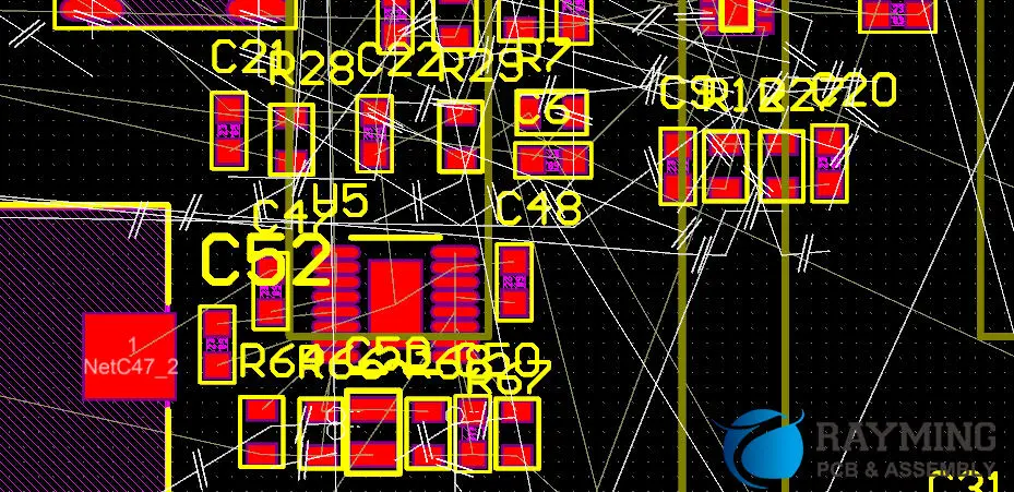
Having all parts dropped means we now need to connect the dots – to make tracks linking parts pins together as electrically defined by our netlist connectivity imported from the schematic. This is the routing stage.
To interactively route:
- Select signal layer intended for trace
- Choose routing tool – track/via/wire
- Click trace start point – say a component pad
- Route trace and click destination pad
- Repeat tracing all points in same signal net
Routing Tips
- Minimize via counts on signal layers
- Use angled traces instead of meanders
- Complete power traces first then signals
- Route one trace end to end before starting next trace
- Think neatness – avoid chaotic board appearance.
Use grid and snap controls to tidy up traces. Switch layers when changing routing direction avoiding collisions. Toggle rats nest view to verify unrouted connections pending.
The goal is to effectively link component pads together using copper track traces layer by layer until the rats nest fully disappears.
Your routed board should perfectly mirror the schematic connectivity down to the physical domain once routing is complete.
Final Checks – DRC, 3D View, Emulate
Before generating manufacturing gerber and drill files, run final checks:
- Design Rule Check – Validate no clearance violations under menu
Tools > Design Rule Check - 3D View – Under
View > 3D Viewervisually check for missed connections in 3D mode - Emulate – Tool
Tools > Generate Footprint Positions Fileexports a.pos3D assembly file from the board to mechanically trial component fit, clearances etc. in a New Project
Fix any last minute minor issues based on the feedback from these validation checks.
Output Gerber and Drill Files
Finally, we are ready to produce manufacturing outputs by plotting gerber masks and drill hits database.
Steps:
- Menu
File > Fabrication Outputs. - Select All layers you want outputs for- Top copper, bottom copper etc.
- Ensure options to generate Drill Map (.drl) file is selected.
- Click
Make Plotsbutton to save gerber files.
Send the Gerber zip file bundle with .drl drill map to your PCB fabrication vendor’s order upload portal or rep to get your designed bare boards manufactured now!
Final Words
And that concludes converting a KiCad schematic drawing down to functional PCB layout ready for fabrication and assembly.
The key concepts covered again:
- Generate netlist connectivity file from schematic capture
- Import this into new PCBnew layout project
- Assign footprints matching schematic symbols
- Follow methodical placement and routing workflow
- Complete design rule checks before output
- Export manufacturing plot gerber and drill data
As you gain proficiency translating schematic circuits to routed boards using the KiCad open source EDA tool suite, your custom PCB realization confidence and speed only gets better through applying these fundamentals incrementally to build experience.
Hope this gives electronics hobbyists, makers and engineers a helpful starter framework to take first concept schematics through to manufacturable layout output systematically using the popular KiCad platform.
Good luck with your next schematic to PCB layout project!
FAQs
What are some key hotkeys useful for PCB Layout in KiCad?
General Navigation
mm– Move origin crosshairJump– Rapidly move canvas to selected object<>– Flip Boarda– Select layer/tool/settingsz– Dynamic zoomg– Toggle grid visibility
Layers & Colors
l– Flip current layerShift+S– Stack colors./,– Next/previous layer
Editing Actions
m– Move footprintr– Rotate footprintf– Flip footprintDel– Delete item
Trace Routing
x– Route track segmentv– Place viaShift– Cycle through available widths. ,– Cycles displayed nets
Consult full KiCad PCB hotkeys list for all shortcuts available.
What’s a good work flow for routing a complex board in KiCad?
For a complex board with high component density and tight clearance requirements, here is an efficient professional routing workflow to follow:
1) Have power input section already defined
2) Place any shield can components first establishing space
3) Grid place groups of same-function parts (ICs, caps etc)
4) Route power buses first on inner layers first
5) Fanout traces from each group keeping same nets together
6) Complete high-speed traces first, minimize vias 7) Use grid to tidy up traces layout iteration by iteration
8) Do most routing on outer layers keeping inner organized
9) Treat every trace uniquely, don’t batch all connects
10) Continually DRC check; validate 3D view for sound assembly
Following the above methodical placement-routing sequence minimizes chaos, rework and ensures optimal board layout quality from complexity perspective.
How do I calculate trace widths in KiCad to handle required current loads?
You can either manually calculate appropriate copper trace widths on PCB to safely carry expected current using factors like:
- Conductor temperature rise
- Base copper thickness
- Maximum current expected
- Ambient temperature considerations
Or simply leverage KiCad’s intuitive built-in PCB calculator to compute minimum widths and spacing.
Steps to use KiCad Trace Width Calculator:
- After placement work, select Menu
Tools > Calculator - Go to tab
PCB Trace Width - Enter variables like Current, Temperature Rise, Copper Weight
- See minimum Trace Width value calculated
This helps quickly validate trace geometries planned are adequately sized to handle power rails current, preventing overheating while being cost effective not over-designing.
What should I do if changes happen to the schematic after routing is complete?
It is common in complex board design that logic modifications or component shuffling happens in schematic even after substantial layout routing has occurred. KiCad has some smart ways to forward-migrate changes:
- For minor component reference designator alterations, use
Swap Referencetool underTools > Referencemenu to rapidly remap parts - For modest connectivity changes, manually edit routed traces to match revised nets
- For major schematic changes, scrap existing work and go back to start – regenerate netlist from new schematic version and re-import to wipe slate clean!
So depending on scope magnitude of ECO changes to base schematic, you can either surgically update final layouts or restart conversion process to resample schematic. Use version control between major iterations.
I hope these additional tips help further demystify practical aspects converting schematic concepts to physical PCB layouts using the KiCad EDA open source software suite.