Panelization is the process of arranging multiple PCB designs into a single panel for efficient manufacturing. This technique reduces production costs, improves manufacturing efficiency, and ensures consistent quality across all boards. Whether you’re a hobbyist or professional PCB designer, understanding proper panelization techniques is crucial for successful PCB production.
The Importance of Proper Panelization
Proper panelization offers several key benefits:
- Cost reduction through optimized material usage
- Improved manufacturing efficiency
- Better quality control
- Reduced handling damage
- Simplified assembly processes

Essential Panelization Parameters

Panel Size Considerations
The standard panel sizes vary depending on your manufacturer’s capabilities and requirements. Here’s a typical breakdown:
| Panel Size (mm) | Common Applications | Typical Board Count | Manufacturing Method |
| 457 x 305 | Large production | 4-12 boards | Automated assembly |
| 305 x 254 | Medium production | 2-8 boards | Mixed assembly |
| 254 x 203 | Small production | 1-4 boards | Manual assembly |
| 152 x 152 | Prototyping | 1-2 boards | Manual assembly |
Board Spacing Requirements
Proper spacing between boards is crucial for successful manufacturing. Here are the recommended specifications:
| Element | Minimum Spacing (mm) | Optimal Spacing (mm) | Maximum Spacing (mm) |
| Board-to-Board | 2 | 3 | 5 |
| Board-to-Edge | 5 | 7.5 | 10 |
| Route Channel | 2 | 2.5 | 3 |
| Fiducial Margin | 5 | 7.5 | 10 |
Step-by-Step Panelization Process
1. Pre-Panelization Preparation
Before starting the panelization process, ensure you have:
- Completed and validated individual PCB designs
- Confirmed manufacturer’s requirements
- Determined production volume
- Selected appropriate panel size
- Gathered necessary design tools
2. Choosing the Right Panelization Method
Mouse-Bite Method
The mouse-bite method uses small routed holes to create break-away tabs. This approach offers:
- Clean separation
- Minimal board edge damage
- Easy manual separation
- Good for both prototype and production runs
V-Score Method
V-scoring creates a groove on both sides of the panel, allowing for easy separation:
- Straight-line breaks only
- Excellent for rectangular boards
- Higher production efficiency
- Better for larger production runs
3. Panel Layout Optimization
Efficiency Calculations
Use this formula to calculate panel efficiency:
| Parameter | Formula | Target Percentage |
| Material Utilization | (Total Board Area / Panel Area) × 100 | > 70% |
| Production Efficiency | (Usable Boards / Total Possible Boards) × 100 | > 90% |
| Waste Factor | (Unused Area / Total Panel Area) × 100 | < 30% |
4. Adding Manufacturing Elements
Required Panel Features
| Feature | Purpose | Placement Guidelines |
| Fiducials | Alignment reference for assembly | Minimum 3 per panel, corners preferred |
| Tooling Holes | Panel handling and registration | 3-4 mm diameter, panel edges |
| Test Coupons | Quality control verification | Panel edges, easy access |
| Panel Rails | Structural support and handling | 5-10 mm width on all sides |
Advanced Panelization Techniques
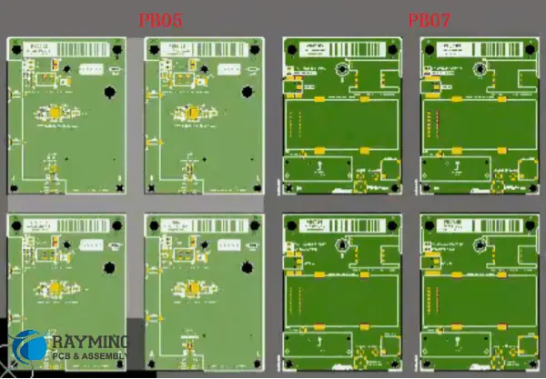
Multi-Design Panels
When panelizing different designs together:
- Group similar thickness boards
- Align similar component heights
- Consider assembly flow
- Maintain consistent orientation
Special Considerations
High-Speed Design Panels
For high-speed circuit boards:
- Maintain impedance control across the panel
- Consider signal integrity requirements
- Use appropriate spacing for sensitive circuits
- Include additional test points
Flexible PCB Panelization
Flexible PCB panelization requires:
- Additional support structures
- Careful handling considerations
- Special attention to bend areas
- Modified break-away methods
Software Tools and Automation
Common Panelization Software
| Software Name | Key Features | Best For |
| CAM350 | Advanced panel optimization | Professional production |
| GenCAD | Basic panelization tools | Small-scale production |
| GerbMerge | Open-source solution | Hobbyist projects |
| PanelizeXpress | Automated panel generation | Medium production runs |
Quality Control and Verification
Pre-Production Checklist
- Verify all design rules
- Check panel dimensions
- Confirm break-away method compatibility
- Validate manufacturing elements
- Review assembly requirements
Common Panelization Errors
| Error Type | Common Causes | Prevention Methods |
| Spacing Issues | Incorrect board-to-board gaps | Use manufacturer templates |
| Missing Features | Overlooked fiducials or tooling holes | Comprehensive checklist |
| Edge Problems | Improper break-away design | Follow material-specific guidelines |
| Layout Errors | Poor optimization | Use automated layout tools |
Frequently Asked Questions
Q1: What is the minimum recommended spacing between PCBs on a panel?
A: The minimum recommended spacing between PCBs is 2.0mm, but optimal spacing is 3.0mm. This ensures proper routing and prevents damage during separation.
Q2: How do I calculate the optimal panel size for my project?
A: Calculate the optimal panel size by:
- Determining individual board dimensions
- Adding required spacing
- Considering manufacturer’s standard panel sizes
- Optimizing for material utilization (aim for >70% efficiency)
Q3: Which break-away method should I choose for my project?
A: Choose based on:
- Mouse-bite: Best for prototypes and complex shapes
- V-score: Ideal for rectangular boards and high-volume production
- Tab-route: Good for mixed-shape panels with moderate production volumes
Q4: How many fiducials should be included on a panel?
A: Include a minimum of three fiducials per panel, placed in a triangular pattern. For larger panels or high-precision assembly, consider adding additional fiducials at strategic locations.
Q5: Can I mix different PCB designs on the same panel?
A: Yes, you can mix different PCB designs on the same panel if they share:
- Similar thickness
- Compatible manufacturing requirements
- Similar assembly processes
- Consistent material specifications
Conclusion
Successful PCB panelization requires careful planning, attention to detail, and understanding of manufacturing requirements. By following these guidelines and best practices, you can optimize your PCB production process, reduce costs, and ensure high-quality results. Remember to always verify your panelization design with your PCB manufacturer before proceeding with production.