The success of printed circuit board (PCB) manufacturing depends heavily on two critical design methodologies: Design for Assembly (DFA) and Design for Manufacturing (DFM). While these terms are often used interchangeably or confused with one another, they represent distinct yet complementary approaches that address different aspects of the PCB production process. Understanding the fundamental differences between DFA and DFM is essential for engineers, designers, and manufacturers who want to optimize their PCB designs for cost-effectiveness, reliability, and manufacturability.

Understanding Design for Manufacturing (DFM)
Design for Manufacturing (DFM) focuses on optimizing the PCB design to make the manufacturing process as efficient, cost-effective, and error-free as possible. DFM principles are applied during the design phase to ensure that the bare PCB can be fabricated successfully using standard manufacturing processes and equipment. The primary goal is to create a design that can be manufactured consistently with high yield rates while minimizing production costs and lead times.
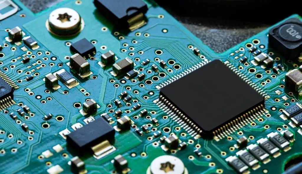
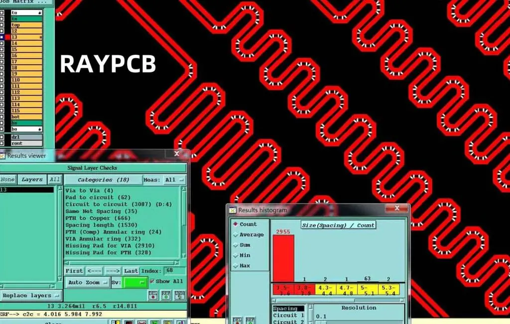
DFM considerations for PCBs encompass various aspects of the bare board fabrication process. Trace width and spacing requirements are fundamental DFM concerns, as they must comply with the capabilities of the chosen PCB fabrication facility. Minimum trace widths, via sizes, and spacing between conductors must be carefully considered to ensure the board can be manufactured reliably. Layer stackup design is another crucial DFM element, where engineers must balance electrical performance requirements with manufacturing constraints such as available prepreg thicknesses and copper weights.
Material selection plays a significant role in DFM optimization. Choosing standard materials and thicknesses that are readily available from PCB manufacturers can significantly reduce costs and lead times compared to exotic or custom materials. Additionally, DFM principles guide decisions about hole sizes, drill aspects ratios, and the placement of vias to ensure they can be reliably drilled and plated during fabrication.
The DFM process also involves considerations for panelization, where multiple PCBs are arranged on a single panel for efficient manufacturing. Proper panel design includes adequate spacing between boards, appropriate tooling holes, and fiducial markers for automated handling equipment. Surface finish selection, such as HASL, ENIG, or OSP, is another DFM consideration that affects both manufacturability and end-use performance.
Understanding Design for Assembly (DFA)
Design for Assembly (DFA) focuses specifically on optimizing the PCB design to facilitate the efficient and reliable assembly of electronic components onto the manufactured board. While DFM addresses the fabrication of the bare PCB, DFA is concerned with the subsequent process of component placement, soldering, and final assembly operations. The primary objective of DFA is to minimize assembly time, reduce assembly costs, improve yield rates, and enhance the overall reliability of the assembled product.
DFA principles heavily influence component selection, placement, and orientation decisions. Component footprint design must accommodate the capabilities of pick-and-place equipment, ensuring that components can be accurately positioned during automated assembly. This includes considerations for component package types, with preference often given to surface-mount devices (SMDs) over through-hole components due to their compatibility with high-speed automated assembly processes.
Solder joint accessibility and inspectability are key DFA concerns. Components must be positioned to allow proper solder joint formation and enable both automated optical inspection (AOI) and manual visual inspection. This involves maintaining adequate spacing between components, avoiding component shadowing that could interfere with inspection processes, and ensuring that critical solder joints remain visible and accessible.
Thermal management during assembly is another important DFA consideration. Large components or heat sinks can create thermal shadows during reflow soldering, potentially leading to poor solder joint formation for nearby components. DFA principles guide the placement of components to ensure uniform heating during the soldering process and may influence decisions about component orientation and spacing.
Test point accessibility represents a crucial DFA element, as assembled boards must often undergo electrical testing. DFA guidelines ensure that test points are properly positioned and accessible to testing equipment, facilitating efficient in-circuit testing and functional verification procedures.
Key Differences in Focus and Scope
The fundamental difference between DFA and DFM lies in their respective focus areas within the PCB production workflow. DFM is primarily concerned with the fabrication of the bare PCB substrate, addressing challenges related to etching, drilling, plating, and other board manufacturing processes. DFA, conversely, focuses on the assembly phase, where electronic components are mounted and soldered onto the fabricated PCB.
This distinction in focus leads to different optimization priorities. DFM optimization typically emphasizes factors such as manufacturability margins, yield improvement in PCB fabrication, and cost reduction in substrate production. DFA optimization prioritizes assembly efficiency, component placement accessibility, soldering reliability, and testing convenience.
The timing of implementation also differs between these approaches. DFM considerations must be addressed early in the design process, as they fundamentally affect the PCB stackup, layer count, material selection, and physical board characteristics. Once the board is fabricated, most DFM-related parameters cannot be changed. DFA considerations, while also best addressed during initial design phases, can sometimes be modified through component selection changes or placement adjustments even after initial board fabrication.
Impact on Design Decisions
DFM and DFA principles often influence different aspects of PCB design decisions, though some overlap exists. DFM heavily influences decisions about copper thickness, dielectric materials, via structures, and minimum feature sizes. These parameters directly affect the PCB fabrication process and must align with the capabilities of the chosen manufacturing facility.
DFA principles primarily influence component selection, placement strategies, and assembly-related design features. This includes decisions about component package types, orientation requirements, spacing constraints, and the inclusion of assembly aids such as fiducial markers and tooling holes.
Sometimes DFM and DFA requirements can conflict, requiring design compromises. For example, DFM might prefer larger via sizes for better manufacturability, while DFA might prefer smaller vias to maximize routing density and component placement flexibility. Successful PCB design requires balancing these potentially competing requirements to achieve an optimal overall solution.
Implementation Strategies
Effective implementation of both DFM and DFA requires close collaboration between design teams and manufacturing partners. DFM implementation typically involves early engagement with PCB fabrication houses to understand their specific capabilities, limitations, and preferences. This collaboration helps establish design rules that align with manufacturing capabilities while meeting electrical and mechanical requirements.
DFA implementation requires similar collaboration with assembly houses, component suppliers, and testing facilities. Understanding the capabilities and limitations of pick-and-place equipment, reflow ovens, and testing systems helps inform design decisions that optimize assembly efficiency and reliability.
Many organizations implement DFM and DFA through formal design review processes, where manufacturing and assembly partners evaluate designs before production begins. These reviews help identify potential issues early in the development cycle when changes are less costly and time-consuming to implement.
Economic Implications
The economic impact of proper DFM and DFA implementation can be substantial. Effective DFM can reduce PCB fabrication costs through improved yields, reduced scrap rates, and shortened production cycles. It can also minimize the need for expensive manufacturing processes or exotic materials, leading to significant cost savings in high-volume production.
Similarly, proper DFA implementation can dramatically reduce assembly costs through faster placement times, higher first-pass yields, and reduced rework requirements. The cumulative effect of small improvements in assembly efficiency can result in significant cost savings when multiplied across thousands or millions of units.
Conclusion
While DFA and DFM are complementary approaches that both contribute to successful PCB production, understanding their distinct focus areas and requirements is essential for optimal design outcomes. DFM addresses the challenges of bare board fabrication, emphasizing manufacturability, yield, and cost optimization in PCB substrate production. DFA focuses on assembly efficiency, component placement optimization, and testing accessibility in the component mounting and soldering phases.
Successful PCB design requires careful consideration of both DFM and DFA principles, often requiring trade-offs and compromises to balance competing requirements. By understanding these differences and implementing both approaches systematically, engineers can create PCB designs that are not only electrically and mechanically sound but also optimized for efficient, cost-effective manufacturing and assembly. The investment in proper DFM and DFA implementation pays dividends through reduced production costs, improved quality, shorter development cycles, and enhanced product reliability in the marketplace.