When talking of PCBs, trace typically deals with a board’s network of fuses, copper, wiring, and insulation. Whenever any electronic equipment malfunctions, then the PCB tracing will most likely be inconsistent. Also, engineers in the PCB field always make use of this phrase “trace resistance” very frequently.
In addition, the trace resistance deals with a board’s components which serve as a barrier to free electricity flow.
What Does Copper Trace PCB Mean?
Every PCB is dependent on the trace. This is similar to the pcb trace current, which is for effective operation. Also, any errors in calculating and detecting the trace would require more effort and time utilized during fitting. In addition, this can make devices or any gadget to have errors, which could be bad for the user.
During the repair or assembling o a printed circuit board, you should be very familiar with the components contained in it coupled with the functions and formulas that will suit your requirements and needs.
Why You Should Use the Copper Trace PCB
One great quality of copper is its great conductivity. This makes sure of the minimal loss of energy during the transmission. Also, manufacturers have what it takes to save much copper when it doesn’t use too much. Standard PCB layouts could use just an ounce of metal to cover one square meter of the substrate with a copper layer with thickness 35 micrometers thick. Also, you can easily get access to copper and it is extremely affordable.
Many capabilities as well as features of PCB s are possible. This is happening due to electricity. These boards’ circuits are just conduits for the proper electric current transport between two different points. This is why their performance is very important. The material of choice is copper due to its high conductivity, although a dozen other materials can transfer electricity as well.
Due to the fact that just one electron is contained in its valence shell or free electron, this copper is known to have a great electron mobility, thereby making it a great conductor. In addition, these electrons feature low barriers to crossing between two atoms. Since the electrons form the basically-charged particles, the free electrons are those responsible for the transmission of electricity. This copper helps in preventing the loss of energy during the impulse transmission.
With all these reasons stated above, the most appropriate material for your PCB traces or traces in PCB is copper.
What is Copper Trace PCB Resistance?
One important aspect you should look into during the PCB design is the traces’ resistance. Resistance is one out of the many qualities that is shared by all the materials in the cosmos. Usually, PCBs make use of copper; however copper comes in different forms, with each form coming with its own drawbacks and benefits. The designing as well as the execution of problems can arise out of the resistance of the PCB tracing. Circuits that are more complicated would definitely experience more problems.
Copper Trace PCB Resistance Calculation
When you apply ohm’s law to a known data, then you can easily determine the tracing resistance. The estimator for the PCB tracing resistance is an in-built feature of the majority of design applications and suite frameworks, which can aid the prediction of the resistance of the copper trace on the board.
Furthermore, this calculator works with an algorithm that is universally applicable in determining the challenge level, thereby guaranteeing that this result would always be the same, regardless of where it is utilized.
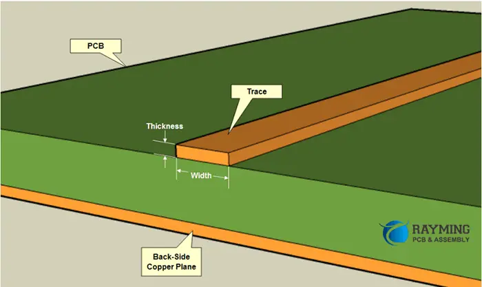
The height, width, and length stand in for the trace’s actual dimensions. This word PCB stands for the resistivity of the materials, whereas this symbol stands for the temperature coefficient of copper. Moreover, these calculations’ results are just approximations. The eventual cost of the material would alter by a minimal amount after the manufacture.
Resistance Calculator for the Copper Trace PCB
Printed circuit boards all make use of some standard formulas. All the tracking resistance would be nowhere to be found if this was an incorrect formula. Not understanding the way the PCB tracing resistance is computed is a well-known error usually made.
Using the Equation for the Copper Trace PCB Resistance

This phenomenon could happen in pcb trace current sensing systems which rely on resistance. This system would read a resistance of 1100 ohms rather than the standard 1000 ohms when one ohm sensing resistor is utilized with a trace of 0.025 mm.
This disparity is a huge one, and it could cause a drop in the currency’s value more than required or even needed. Also, manipulating the PCB trace thickness and width without working with some complex math is possible. Rather than calculate the PCB trace width, you may need to consider the alternatives.
If you wish to know the circuits’ properly associated with them, you can handle the first just by observing what the width is as well as raise or decrease it. This would accomplish different things. The first being that it would help in expanding the area of copper, offering additional wiggle room so as to try different resistance values out. Secondly, it would reduce the resistance of copper on the board. In addition, it would give more room for the testing to be able to establish the right trace width.
Why You Should Calculate the Copper Trace PCB Thickness
Simple procedures or calculations might not detect trace resistance accurately. Also, calculating the PCB trace might not be accurate or enough. Moreover, with an accurate calculation of the copper trace PCB thickness as well as the trace, is necessary to ensure the PCB traces’ proper activation. Any given resistance of the PCB trace could be reduced through the calculation as well as increasing the trace’s width considerably.
Conclusion
Printed circuit boards are known to form the base and skeleton of many electronic devices and gadgets. When planning your printed circuit board, these are the things you must put in place. Every PCB is dependent on the trace. This is similar to the pcb trace current, which is for effective operation. Also, any errors in calculating and detecting the trace would require more effort and time utilized during fitting.