Introduction
In the realm of printed circuit board (PCB) assembly, quality assurance and fault detection are paramount concerns. As electronic systems become increasingly complex and densely integrated, traditional testing methods often fall short in providing comprehensive coverage and accessibility. This is where boundary-scan testing emerges as a powerful solution, offering numerous benefits that streamline the manufacturing process, enhance quality control, and ultimately improve the overall reliability of electronic products.
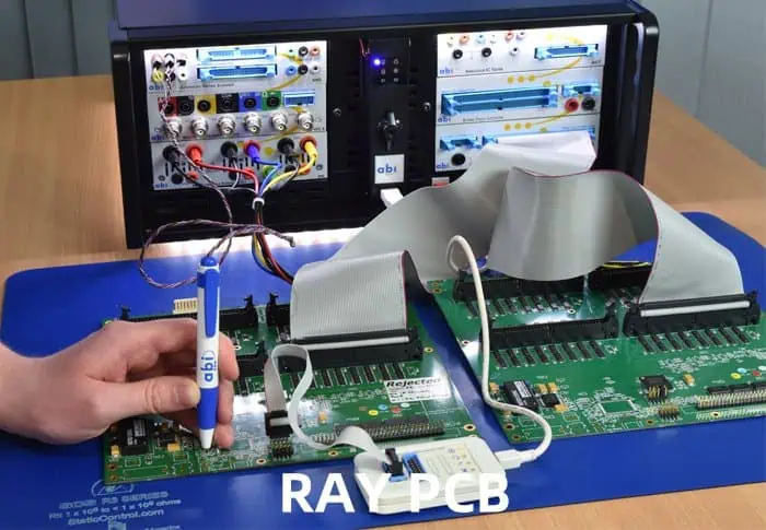
Boundary-scan testing, also known as JTAG (Joint Test Action Group) testing, is a standardized methodology that utilizes specialized hardware and software to test interconnections, components, and functionality on PCBs. This article delves into the advantages of boundary-scan testing and how it can significantly enhance the PCB assembly process.
Understanding Boundary-Scan Testing
Boundary-scan testing is based on the IEEE 1149.1 standard, which defines a set of rules and protocols for testing interconnections and components on PCBs. The core concept revolves around incorporating specialized test logic, known as boundary-scan cells, into integrated circuits (ICs) during their design phase.
These boundary-scan cells act as controllable input/output points, allowing for the testing of interconnections between ICs and other components on the PCB. By leveraging these dedicated test points, boundary-scan testing can access and control individual pins or nodes on the PCB, enabling comprehensive testing and fault isolation capabilities.
Benefits of Boundary-Scan Testing for PCB Assembly
Boundary-scan testing offers numerous advantages that make it an invaluable tool for PCB assembly and quality assurance processes. Here are some of the key benefits:
1. Improved Test Coverage and Accessibility
Traditional testing methods, such as bed-of-nails fixtures or flying probe testers, often struggle to access dense and complex PCB designs with buried or inaccessible nodes. Boundary-scan testing overcomes this limitation by utilizing the dedicated test logic built into the ICs themselves, providing access to virtually every node on the PCB, including those that are physically inaccessible or buried beneath components.
2. Enhanced Fault Detection and Diagnostics
Boundary-scan testing allows for precise fault detection and diagnostics at the interconnection level. By controlling and monitoring individual pins and nodes, boundary-scan testing can identify open circuits, short circuits, and other interconnection-related defects with high accuracy. This level of granularity in fault detection enables more efficient root cause analysis and targeted repair or rework efforts.
3. Reduced Manufacturing Costs
By incorporating boundary-scan testing into the PCB assembly process, manufacturers can significantly reduce overall manufacturing costs. Improved test coverage and fault detection capabilities lead to fewer defective products reaching the end-user, reducing the need for costly field repairs or replacements. Additionally, boundary-scan testing can help streamline the manufacturing process by eliminating the need for complex and expensive test fixtures or probing systems.
4. Improved Product Quality and Reliability
Boundary-scan testing plays a crucial role in ensuring product quality and reliability. By thoroughly testing interconnections and components during the manufacturing process, potential defects or issues can be identified and addressed before the product reaches the customer. This proactive approach to quality assurance helps to minimize the risk of field failures and enhances overall product reliability.
5. Faster Time-to-Market
The efficiency and effectiveness of boundary-scan testing can contribute to faster time-to-market for new products. By streamlining the testing and debugging processes, manufacturers can shorten the overall development and production cycles, enabling them to bring their products to market more quickly while maintaining high quality standards.
6. Compliance with Industry Standards and Regulations
Many industries, such as aerospace, automotive, and medical electronics, have strict quality and safety regulations in place. Boundary-scan testing can help manufacturers comply with these standards by providing comprehensive testing and documentation capabilities. The IEEE 1149.1 standard itself is widely recognized and accepted across various industries, further reinforcing the credibility and compliance of boundary-scan testing.
Implementing Boundary-Scan Testing
To effectively implement boundary-scan testing in the PCB assembly process, manufacturers should consider the following steps:
- IC Selection: Choose ICs that support boundary-scan testing and comply with the IEEE 1149.1 standard. Many modern ICs, particularly those used in complex designs, are equipped with boundary-scan capabilities.
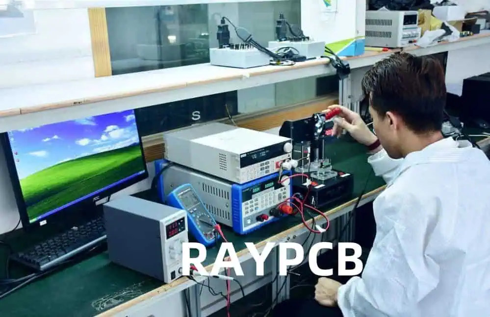
- Test Development: Develop comprehensive test programs and procedures specific to the PCB design. This may involve leveraging boundary-scan test development tools and creating test patterns tailored to the interconnections and components on the PCB.
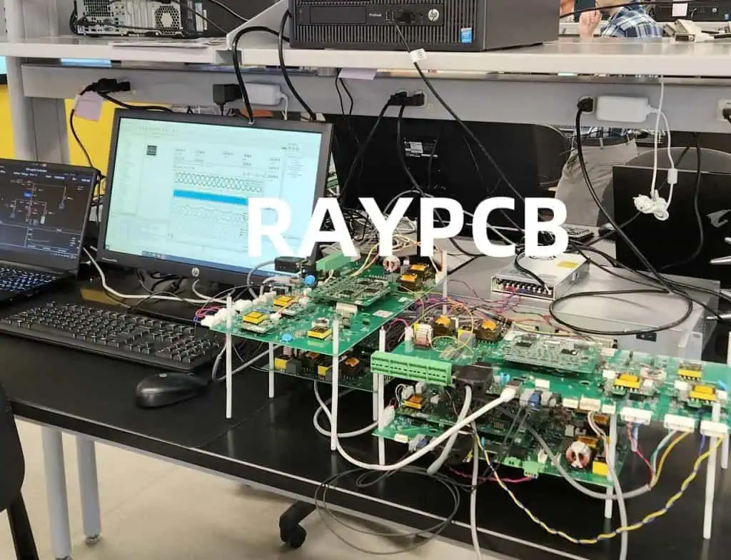
- Test Integration: Integrate boundary-scan testing into the overall manufacturing and quality assurance processes. This may involve incorporating dedicated boundary-scan test equipment or integrating boundary-scan testing with existing test platforms.
- Training and Expertise: Ensure that appropriate training and expertise are available within the manufacturing team. Boundary-scan testing requires specialized knowledge and skills to effectively develop, execute, and interpret test results.
- Continuous Improvement: Continuously monitor and optimize the boundary-scan testing process. Regularly review test coverage, fault detection rates, and overall effectiveness to identify areas for improvement and adapt to evolving product designs and manufacturing requirements.
Data Visualization
To better illustrate the benefits of boundary-scan testing, let’s consider the following tables:
Table 1: Test Coverage Comparison
| Testing Method | Test Coverage |
|---|---|
| Bed-of-Nails | 60-80% |
| Flying Probe | 70-90% |
| Boundary-Scan | 95-99% |
This table compares the test coverage achieved by different testing methods. Boundary-scan testing offers significantly higher test coverage, ranging from 95% to 99%, compared to traditional methods like bed-of-nails or flying probe testers, which typically achieve lower coverage rates.
Table 2: Defect Detection and Yield Improvement
| Testing Method | Defect Detection Rate | Yield Improvement |
|---|---|---|
| No Testing | – | – |
| Traditional Methods | 60-80% | 10-20% |
| Boundary-Scan | 90-98% | 25-35% |
This table illustrates the impact of different testing methods on defect detection rates and yield improvement. Boundary-scan testing can achieve defect detection rates of 90-98%, significantly higher than traditional methods. Consequently, boundary-scan testing can lead to yield improvements of 25-35%, resulting in substantial cost savings and improved product quality.
Table 3: Cost Savings with Boundary-Scan Testing
| Cost Factor | Potential Savings |
|---|---|
| Reduced Test Fixtures | 10-20% |
| Reduced Field Returns/Repairs | 15-25% |
| Increased Manufacturing Yield | 5-15% |
| Streamlined Debug and Rework | 10-20% |
This table outlines the potential cost savings associated with implementing boundary-scan testing in the PCB assembly process. By reducing the need for expensive test fixtures, minimizing field returns and repairs, increasing manufacturing yield, and streamlining debug and rework processes, boundary-scan testing can contribute to significant cost savings across various areas of the manufacturing lifecycle.
These tables provide a visual representation of the advantages of boundary-scan testing, highlighting its superior test coverage, improved defect detection capabilities, and potential cost savings compared to traditional testing methods.
Frequently Asked Questions (FAQs)
- What is the difference between boundary-scan testing and traditional testing methods? Traditional testing methods, such as bed-of-nails fixtures or flying probe testers, access and test PCBs from the outside, often facing limitations in reaching buried or inaccessible nodes. In contrast, boundary-scan testing utilizes dedicated test logic built into the ICs themselves, allowing for comprehensive testing of interconnections and components, including those that are physically inaccessible.
- How does boundary-scan testing improve fault detection and diagnostics? Boundary-scan testing enables precise fault detection and diagnostics at the interconnection level. By controlling and monitoring individual pins and nodes, boundary-scan testing can identify open circuits, short circuits, and other interconnection-related defects with high accuracy. This level of granularity in fault detection facilitates more efficient root cause analysis and targeted repair or rework efforts.
- What are the benefits of boundary-scan testing in terms of cost savings? Boundary-scan testing can contribute to significant cost savings in various areas of the manufacturing process. It reduces the need for expensive test fixtures, minimizes field returns and repairs, increases manufacturing yield, and streamlines debug and rework processes. These cost savings can range from 10-25% across different cost factors.
- How does boundary-scan testing improve product quality and reliability? By thoroughly testing interconnections and components during the manufacturing process, boundary-scan testing helps identify and address potential defects or issues before the product reaches the customer. This proactive approach to quality assurance minimizes the