The electronics industry is experiencing a revolutionary transformation, driven by the demand for smaller, more efficient, and increasingly complex devices. At the heart of this evolution lies 3D-MID (Molded Interconnect Device) technology, also known as 3D Circuits, which is reshaping how we design and manufacture everything from smartphones to advanced robotics systems. This innovative approach to circuit integration is not just changing the game—it’s redefining the entire playing field.

Understanding 3D-MID Technology: The Foundation of Modern Electronics
3D-MID technology represents a paradigm shift from traditional flat circuit boards to three-dimensional electronic structures. Unlike conventional PCBs (Printed Circuit Boards) that are typically flat and require separate mechanical housings, 3D-MID combines the circuit carrier and mechanical structure into a single, integrated component. This revolutionary approach creates 3D circuits that can be molded into virtually any shape, enabling unprecedented design flexibility and functionality.
The technology works by creating a plastic substrate using injection molding, followed by selective metallization to create conductive pathways. These pathways form the electrical connections necessary for component mounting and signal transmission. The result is a single component that serves both as the mechanical structure and the electrical circuit, eliminating the need for separate housing and interconnection components.
The 3D-MID Manufacturing Process: Precision Meets Innovation
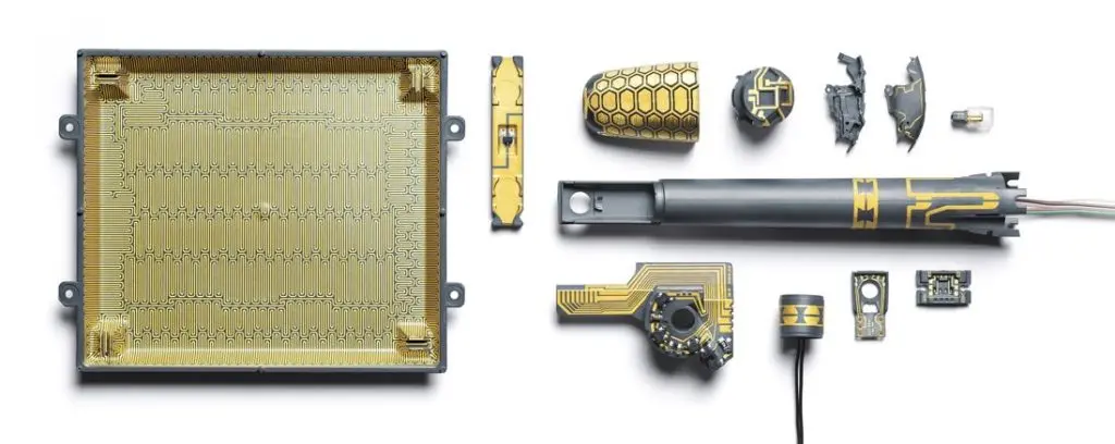
The creation of 3D circuits involves several sophisticated manufacturing steps that showcase the technology’s precision and versatility. The process begins with injection molding using thermoplastic materials that have been specially formulated for electronic applications. These materials must possess excellent electrical properties, dimensional stability, and the ability to withstand the subsequent metallization processes.
During the molding phase, specific areas of the plastic substrate are designed to become conductive pathways. This is achieved through various techniques, including laser direct structuring (LDS), two-shot molding, or masking and etching processes. The LDS method, in particular, has gained significant traction due to its precision and efficiency. It involves adding a metal-plastic additive to the base material, which is then activated by laser treatment to create selective metallization areas.
Following the structural formation, the metallization process creates the actual 3D circuits. This typically involves electroless plating, where copper and other metals are deposited onto the activated areas. The result is a robust, reliable electrical pathway that can handle the demanding requirements of modern electronic devices.
Revolutionizing Smartphone Design with 3D-MID
The smartphone industry has been one of the earliest and most enthusiastic adopters of 3D-MID technology. As consumers demand thinner, lighter, and more feature-rich devices, traditional manufacturing approaches have reached their limits. 3D circuits provide the solution by enabling radical miniaturization while maintaining or even improving functionality.
In modern smartphones, 3D-MID components serve multiple critical functions. Antenna systems represent one of the most significant applications, where the technology enables the integration of multiple antennas—including Wi-Fi, Bluetooth, cellular, and NFC—into compact, three-dimensional structures. These 3D circuits can be shaped to fit perfectly within the available space while optimizing signal performance and reducing interference between different communication systems.
Camera modules in smartphones also benefit tremendously from 3D-MID technology. The complex mechanical and electrical requirements of modern camera systems, including autofocus mechanisms, image stabilization, and multiple lens configurations, can be integrated into single 3D circuit components. This integration not only saves space but also improves reliability by reducing the number of interconnections and potential failure points.
Furthermore, sensor integration has been revolutionized by 3D-MID technology. Accelerometers, gyroscopes, magnetometers, and other sensors can be mounted directly onto 3D circuits that are specifically shaped to optimize their performance and position within the device. This level of integration was simply impossible with traditional flat PCB designs.
Robotics: Where 3D-MID Technology Truly Shines
The robotics industry represents perhaps the most exciting frontier for 3D-MID applications. Robots require complex electronic systems that must fit within articulated joints, curved surfaces, and confined spaces—requirements that are perfectly suited to 3D circuits technology.
In robotic arms and manipulators, 3D-MID components enable the integration of sensors, actuators, and control electronics directly into the mechanical structure. This integration eliminates bulky cable harnesses and separate control boxes, resulting in more agile, responsive, and reliable robotic systems. The ability to create 3D circuits that conform to the exact shape of robotic joints and linkages opens up entirely new possibilities for robot design.
Humanoid robots particularly benefit from 3D-MID technology. The complex curves and contours of human-like forms can be perfectly matched with 3D circuits that provide the necessary electronic functionality while maintaining the desired aesthetic and ergonomic properties. Sensors for touch, pressure, temperature, and position can be seamlessly integrated into the robot’s “skin,” creating more natural and intuitive human-robot interactions.
Autonomous vehicles and drones represent another significant application area for 3D circuits. These systems require numerous sensors, communication devices, and control electronics that must be integrated into aerodynamic and space-constrained designs. 3D-MID technology enables the creation of conformal electronic systems that can be embedded directly into vehicle bodies and wing structures.
Advantages of 3D-MID Over Traditional Electronics Manufacturing
The transition to 3D-MID technology offers numerous compelling advantages over traditional electronics manufacturing approaches. Space efficiency stands as perhaps the most significant benefit, with 3D circuits typically requiring 60-80% less volume than equivalent flat PCB implementations. This dramatic space savings enables entirely new product categories and form factors that were previously impossible.
Weight reduction is another crucial advantage, particularly important in aerospace, automotive, and mobile applications. By eliminating separate mechanical housings and reducing the need for interconnection hardware, 3D-MID components can achieve weight savings of 40-70% compared to traditional designs.
Reliability improvements are equally impressive. 3D circuits reduce the number of solder joints, connectors, and cable assemblies—all potential failure points in electronic systems. The integrated nature of 3D-MID technology creates more robust systems that can better withstand vibration, thermal cycling, and mechanical stress.
Cost considerations also favor 3D-MID technology, particularly in high-volume applications. While the initial tooling costs may be higher, the elimination of assembly steps, reduced material usage, and improved yields often result in lower overall manufacturing costs. Additionally, the reduced testing and quality control requirements for integrated 3D circuits contribute to further cost savings.
Emerging Applications and Future Possibilities
The potential applications for 3D-MID technology continue to expand as engineers and designers recognize the possibilities offered by 3D circuits. The medical device industry is embracing this technology for implantable devices, wearable health monitors, and surgical instruments where space constraints and biocompatibility are critical factors.
Automotive applications are rapidly growing, with 3D circuits being integrated into everything from advanced driver assistance systems to electric vehicle charging infrastructure. The ability to create conformal electronic systems that can be embedded directly into vehicle structures opens up new possibilities for sensor integration and system optimization.
The Internet of Things (IoT) represents another significant growth area for 3D-MID technology. The requirements for small, efficient, and cost-effective connected devices align perfectly with the capabilities of 3D circuits. Smart home devices, industrial sensors, and environmental monitoring systems all benefit from the integration possibilities offered by this technology.
Challenges and Considerations in 3D-MID Implementation
Despite its numerous advantages, 3D-MID technology does present certain challenges that must be carefully considered during implementation. Design complexity is significantly higher than traditional PCB design, requiring specialized software tools and expertise in three-dimensional circuit layout. Engineers must consider not only electrical performance but also mechanical stress, thermal management, and manufacturing constraints in three dimensions.
Material selection becomes more critical with 3D circuits, as the plastic substrate must provide both mechanical strength and electrical performance. The thermal expansion characteristics, chemical compatibility, and long-term stability of the materials directly impact the reliability and performance of the final product.
Manufacturing tolerances are also more challenging to achieve with 3D-MID technology. The three-dimensional nature of the components requires precise control over multiple geometric parameters, and the metallization process must provide consistent electrical properties across complex surfaces.
The Future of 3D-MID Technology
Looking ahead, 3D-MID technology is poised for continued growth and innovation. Advances in materials science are enabling higher performance substrates with improved electrical and mechanical properties. New metallization techniques are providing better adhesion, conductivity, and reliability for 3D circuits.
The integration of active components directly into 3D-MID structures represents an exciting frontier. Research into conductive polymers, printed electronics, and embedded semiconductors could enable 3D circuits that incorporate not just passive interconnections but active electronic functions as well.
Machine learning and artificial intelligence are also being applied to 3D-MID design optimization, enabling automated design tools that can optimize both electrical and mechanical performance simultaneously. These advances will make 3D circuits more accessible to a broader range of engineers and applications.
Conclusion: The 3D-MID Revolution
3D-MID technology represents more than just an incremental improvement in electronics manufacturing—it’s a fundamental shift that enables entirely new approaches to product design and functionality. From the smartphones in our pockets to the robots that will shape our future, 3D circuits are becoming the backbone of next-generation devices.
As the technology continues to mature and costs decrease, we can expect to see 3D-MID applications proliferate across virtually every industry that relies on electronic systems. The ability to create truly three-dimensional electronic structures that integrate mechanical and electrical functions will continue to drive innovation and enable products that were previously impossible to imagine.
The future belongs to 3D circuits, and that future is arriving faster than ever before. Organizations that embrace 3D-MID technology today will be best positioned to lead tomorrow’s technological revolution.