Introduction
In the ever-evolving landscape of modern electronics, integrated circuits (ICs) stand as the cornerstone of technological progress. These miniature marvels, often no larger than a fingernail, are the brains behind our smartphones, computers, and countless other devices that power our digital world. At the heart of bringing these complex components to life lies the crucial process of integrated circuit assembly.
Integrated circuit assembly is the intricate art and science of transforming raw semiconductor materials into functional electronic components. This process involves a series of precise steps, each critical to ensuring the performance, reliability, and longevity of the final product. As technology continues to advance at a breakneck pace, the techniques and innovations in IC assembly play an increasingly vital role in shaping the future of electronics.

This article aims to explore the key techniques, recent innovations, and future trends in integrated circuit assembly. By delving into both traditional methods and cutting-edge advancements, we’ll uncover how this field is pushing the boundaries of what’s possible in electronic design and manufacturing.
Understanding Integrated Circuit Assembly
Definition and Scope
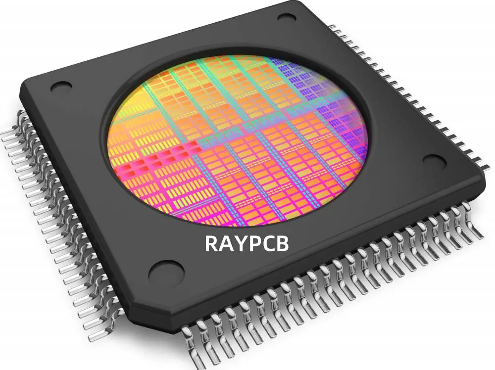
Integrated circuit assembly refers to the process of packaging a semiconductor die (chip) into a functional IC package. This process transforms a bare silicon chip into a protected, usable component that can be integrated into electronic devices. The scope of IC assembly encompasses everything from preparing the die to final testing of the packaged chip.
Overview of Assembly Stages
The integrated circuit assembly process can be broadly divided into four main stages:
- Die Preparation: This involves separating individual dies from the processed wafer and preparing them for packaging.
- Bonding: The die is attached to the package substrate and electrical connections are made between the die and the package leads.
- Packaging: The assembled die is encapsulated in a protective material to shield it from environmental factors and physical damage.
- Testing: The packaged IC undergoes rigorous testing to ensure functionality and reliability.
Key Materials Used in IC Assembly
Several crucial materials are employed throughout the IC assembly process:
- Substrates: Typically made of materials like ceramic, plastic, or glass, these serve as the base for the IC package.
- Adhesives: Used to attach the die to the substrate.
- Bonding wires: Usually gold or copper, these create electrical connections between the die and package leads.
- Encapsulants: Protective materials that surround the die and internal connections.
- Solder: Used for creating external connections on the package.
Traditional Techniques in IC Assembly
Wire Bonding
Wire bonding is one of the most widely used techniques in IC assembly. It involves creating electrical connections between the die and the package leads using thin wires, typically made of gold or copper.
Types of Wire Bonding
- Ball bonding
- Wedge bonding
Advantages
- Flexible and adaptable to different package types
- Well-established technology with high reliability
- Cost-effective for many applications
Flip-Chip Bonding
Flip-chip bonding, also known as controlled collapse chip connection (C4), involves flipping the chip upside down and directly connecting it to the substrate using solder bumps.
Key Features
- Direct die-to-substrate connection
- Higher performance due to shorter electrical paths
- Better heat dissipation
Wafer-Level Packaging
Wafer-level packaging (WLP) is a technique where the IC packaging is done at the wafer level, before the individual chips are separated.
Benefits
- Smaller package size, approaching chip scale
- Improved electrical performance
- Cost-effective for high-volume production
Limitations of Conventional Approaches
While these traditional techniques have served the industry well, they face limitations in meeting the demands of modern electronics:
- Challenges in achieving extremely fine pitches
- Thermal management issues in high-performance applications
- Difficulties in integrating heterogeneous components
Innovations and Emerging Techniques
As the electronics industry pushes for smaller, faster, and more powerful devices, new techniques in integrated circuit assembly have emerged to meet these challenges.
3D Integrated Circuits (3D ICs)
3D ICs represent a significant leap forward in IC assembly, allowing for vertical stacking of multiple dies.
Through-Silicon Vias (TSVs)
TSVs are a key enabling technology for 3D ICs. These are vertical electrical connections that pass through a silicon wafer or die, allowing for direct connections between stacked layers.
Benefits for Performance and Miniaturization
- Reduced signal delay and power consumption
- Higher bandwidth between different functional blocks
- Significant reduction in overall package size
System-in-Package (SiP) Technology
SiP technology takes integration a step further by combining multiple ICs and other components into a single package.
Integration of Heterogeneous Components
SiP allows for the integration of different types of chips and components, such as:
This level of integration enables more compact and powerful electronic systems, crucial for applications like smartphones and IoT devices.
Fan-Out Wafer-Level Packaging (FOWLP)
FOWLP is an advanced wafer-level packaging technique that extends the benefits of WLP to chips with a higher number of I/O connections.
Improved Thermal and Electrical Performance
- Better heat dissipation due to larger package area
- Shorter electrical paths leading to improved signal integrity
- Ability to integrate more I/Os in a smaller form factor
Advanced Materials and Processes
The quest for improved performance has led to the development and adoption of new materials and processes in IC assembly.
Use of Low-k Dielectrics
Low-k dielectric materials are being increasingly used to reduce signal delay and power consumption in high-performance ICs.
New Solder Materials
Lead-free solder alloys and copper pillar bumps are being adopted to meet environmental regulations and improve electrical and thermal performance.
AI-based Inspection Tools
Artificial intelligence and machine learning are being employed in inspection and quality control processes, improving defect detection and yield rates.
Read more about:
Automation and Smart Manufacturing
The integration of advanced automation and smart manufacturing techniques is revolutionizing IC assembly processes.
Role of Robotics and AI in IC Assembly Lines
Robotic systems, guided by sophisticated AI algorithms, are increasingly taking over precision tasks in IC assembly:
- Die placement and alignment
- Wire bonding
- Encapsulation and molding
These systems offer unprecedented levels of accuracy and consistency, crucial for assembling today’s complex ICs.
Quality Control through Machine Learning and Computer Vision
Advanced machine learning algorithms and computer vision systems are being employed to:
- Detect microscopic defects in real-time
- Predict potential failures before they occur
- Optimize process parameters on-the-fly
Benefits: Precision, Yield Improvement, Cost Reduction
The adoption of smart manufacturing techniques in IC assembly offers several key benefits:
- Improved precision in assembly processes
- Significant increases in yield rates
- Reduction in manufacturing costs through increased efficiency and reduced waste
Challenges in Modern Integrated Circuit Assembly
Despite the advancements, the field of IC assembly faces several significant challenges.
Miniaturization and Thermal Management
As ICs continue to shrink while packing in more transistors, two major challenges emerge:
- Achieving finer pitches: The need for increasingly fine pitches in interconnects poses significant technical challenges.
- Heat dissipation: Smaller packages with higher power densities make thermal management a critical concern.
Cost Pressures and Time-to-Market Demands
The electronics industry’s competitive nature puts immense pressure on manufacturers to:
- Reduce production costs
- Shorten development cycles
- Bring products to market faster
These demands often conflict with the need for reliability and quality, creating a delicate balancing act for IC assembly processes.
Environmental and Regulatory Concerns
The IC assembly industry must navigate an increasingly complex regulatory landscape:
- RoHS compliance: Ensuring products are free from hazardous substances like lead.
- Lead-free requirements: Developing and implementing lead-free soldering processes.
- Sustainability: Addressing the environmental impact of manufacturing processes and materials.
Future Trends in IC Assembly
The future of integrated circuit assembly promises exciting developments and challenges.
Quantum and Neuromorphic Chip Assembly Requirements
As quantum computing and neuromorphic chips move from research to practical applications, they will require novel assembly techniques:
- Ultra-low temperature packaging for quantum chips
- High-density, 3D interconnects for neuromorphic systems
Sustainable Assembly Technologies
The push for sustainability is driving research into:
- Biodegradable packaging materials
- Energy-efficient assembly processes
- Improved recycling techniques for electronic components
Integration with Advanced Packaging
The lines between IC assembly and advanced packaging continue to blur, with trends like:
- Chiplets: Assembling systems from smaller, reusable chip components
- Interposers: Using silicon or organic interposers for high-density interconnects
- Embedded die technology: Integrating bare dies directly into PCBs or flexible substrates
Applications Across Industries
The innovations in integrated circuit assembly are enabling advancements across various industries.
Consumer Electronics
In the realm of consumer electronics, advanced IC assembly techniques are enabling:
- Slimmer, more powerful smartphones
- Compact and feature-rich wearable devices
- High-performance gaming consoles and VR headsets
Automotive Electronics
The automotive industry is benefiting from IC assembly innovations in areas such as:
- Advanced Driver Assistance Systems (ADAS)
- Electric Vehicle (EV) control systems
- In-vehicle infotainment and connectivity solutions
Medical Devices and IoT
In healthcare and the Internet of Things, IC assembly advancements are facilitating:
- Miniaturized implantable medical devices
- Wearable health monitors with extended battery life
- Low-power, long-range IoT sensors and devices
Aerospace and Defense
The aerospace and defense sectors leverage cutting-edge IC assembly for:
- High-reliability avionics systems
- Advanced radar and communication equipment
- Radiation-hardened components for space applications
Conclusion
The field of integrated circuit assembly stands at the forefront of technological innovation, continuously pushing the boundaries of what’s possible in electronic design and manufacturing. From traditional wire bonding techniques to cutting-edge 3D IC technologies, the evolution of IC assembly has been nothing short of remarkable.
As we’ve explored in this article, recent innovations like 3D ICs, advanced packaging techniques, and smart manufacturing processes are reshaping the landscape of electronics manufacturing. These advancements are not only meeting the demands for smaller, faster, and more powerful devices but also addressing critical challenges in thermal management, cost reduction, and environmental sustainability.
Looking ahead, the role of integrated circuit assembly in next-generation electronics is set to become even more crucial. As we venture into the realms of quantum computing, neuromorphic systems, and beyond, IC assembly techniques will need to evolve to meet these new challenges. The integration of AI, advanced materials, and sustainable practices will undoubtedly play a significant role in shaping the future of this field.
The journey of innovation in IC assembly is far from over. It calls for continued research, industry collaboration, and a relentless pursuit of technological excellence. As we stand on the brink of new frontiers in electronics, the advancements in integrated circuit assembly will continue to be a driving force, enabling the technologies that will define our future.