Since 2005 we are committed to superior quality and customer service with the highest standards to meet customers requirement and satisfaction

Trusted by more than 10,000 Electronic Engineers
More Than 6,000 Electronic Contract Customers
99.8% satisfied Projects from end Customers
High Frequency materials options: Rogers Arlon Isola Teflon Dupont Taconic Shengyi ...
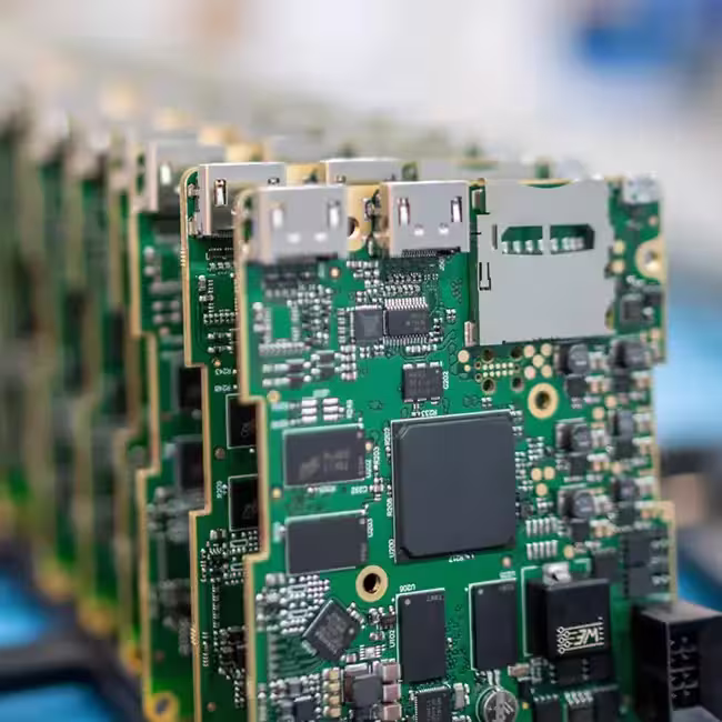
Solutions


I’ve been using RAYPCB over 5 years now, and just like all the projects I’ve done with RAYPCB, there were no surprises. Everything went just as it was supposed to, and the PCB boards is performing fine. You’re lucky to work for such a great company. In my experience it’s very rare to find the kind of competence and compassion that RAYPCB has. You might find one, or the other, but not both. Very rare. Anyway thanks again, if I could I would be working with RAYPCB every day.
John Joseph VP of Product DevelopmentRayMing PCB delivered exceptional quality for our lithium-ion battery management system. Their expertise in thermal management, current handling, and battery protection circuitry was outstanding. The PCBs performed flawlessly under extreme testing conditions with zero defects in production. Fast delivery and excellent technical support made them our go-to partner for critical battery applications.
Michael Senior Hardware EngineerWe developed a special PCB, 4 Layer with cross blind and buried vias. 2oz/3oz/3oz/2oz, 3.0mm thickness, the key difficult is the size: 640.51*796mm, we inquired a lot of PCB companies, they said no to Us, and finally found RAYMING, they decided to assist us as a R&D Project, and finally in the RAYMING 3 months of hard work, they successfully delivered the board, after testing everything is perfect, thank you very much for RAYMING's assistance!
Craig R. William R&D DepartmentWe chose RAYMING PCB because they offer the entire service from PCB manufacturing through to ordering parts, assembling and testing. Compared with other manufactures, we appreciate RAYMING is really communicative during the whole production process. Possible issues are discussed and solved immediately. Hence, we received high quality PCBs with negligible reject rate. In the end RAYMING offers attractive prices, considering the offered services.
Megan Schauf PurchaserIn the medical device industry, there's no room for error. RayMing's rigorous quality control and compliance with industry standards made them the perfect partner for our critical applications. Their team doesn't just manufacture - they collaborate, offering valuable design feedback that improved our product's reliability and reduced our overall costs.
Dr. Amanda Park Product ManagerRayMing Technology was able to match our requirements fully and rapidly for a custom-made solution, specifically to our needs for quick turn Prototype boards. Our company expanded extremely quickly and it was a primary challenge for us to provide highly reliable rigid flex PCB for our system. RAYMING was punctual with the full turnkey services and made deliveries just in time,and were also very responsive to our queries. Eventually, we chose RAYMING. to be our Full-Turnkey Assembly provider. Regards.
Di Meglio R&D ManagerLisa, Thank you so much for the timely delivery of the assembled boards. I’m very pleased with the quality, and the board were already brought up successfully and passed our manufacturing tests! We are very comfortable in placing our next production run with you guys in 2-3 weeks time.
Belle tenue taille Electronic EngineerWe are a very small company and our annual PCB requirements are very small, thanks to RAYMING's support for more than 10 years.
Androsk OwnerRayMing PCB has been instrumental in bringing our IoT products to market. Their attention to detail in PCB fabrication and assembly is exceptional. What sets them apart is their proactive communication throughout the entire process - they catch potential issues before they become problems. Our prototype turnaround time decreased by 40% since partnering with them.
Ahmed Elshikh Engineering DirectorI found RAYMING from google search in 2015, I needed to expedite the production of a sample, RayMing delivered the PCB in time, thank you very much for the support of RAYMING for nearly 10 years, and thank you very much for Stan's very good service. We will continue to order from RAYMING, and hope that RAYMING will continue to maintain high quality delivery and reasonable price.
Jennifer Vasquez Procurement ManagerRayPCB delivered exceptional results for our 5G antenna project. Their material recommendations were spot-on - suggesting Rogers RO4350B for our high-frequency application saved us both cost and performance headaches. The manufacturing quality exceeded our expectations, and their comprehensive testing validated every specification. Turn-around time was impressive too.
Sarah RF EngineerWe've worked with several contract manufacturers, but RayMing's combination of quality and cost-effectiveness is unmatched. Their ISO-certified processes give us confidence in every batch, and their flexible production scaling has supported us through both prototyping and full production runs. They truly understand the challenges of bringing electronic products to market.
Tommy B CTOAs a startup, we needed a manufacturing partner who could grow with us. RayMing provided competitive pricing for our small initial orders while maintaining the capability to scale when we hit our growth targets. Their technical support team helped optimize our designs for manufacturability, saving us both time and money.
James Thompson Founder
RayMing PCB delivered exactly what we needed for our wearable device. Their flexible PCBs handled thousands of bend cycles without any issues, and the ultra-thin design fit perfectly in our compact smartwatch housing. The 3-day turnaround was impressive, and their engineering team provided helpful design suggestions that improved our product's reliability. Quality was consistent across our entire 5,000-unit production run. Excellent communication, competitive pricing, and reliable flexible circuits - exactly what you want in a PCB partner for wearable electronics.
Mike Rodriguez Product Engineer