Printed Circuit Board (PCB) reliability is fundamental to the success of any electronic product. Whether designing consumer electronics, automotive systems, or critical infrastructure equipment, engineers must prioritize reliability from the earliest design phases through manufacturing and deployment. A reliable PCB ensures consistent performance, reduces warranty costs, and maintains customer trust while minimizing field failures that can be costly and dangerous.
Understanding PCB Reliability Fundamentals
PCB reliability encompasses the board’s ability to perform its intended function without failure over its expected operational lifetime under specified environmental conditions. Reliability failures can manifest as intermittent connections, complete circuit failure, component degradation, or physical board damage. These failures often result from thermal stress, moisture ingress, mechanical fatigue, electrical overstress, or manufacturing defects that compound over time.
The key to reliable PCB design lies in understanding failure mechanisms and implementing preventive measures during design, material selection, manufacturing, and testing phases. Reliability engineering requires a systematic approach that considers the entire product lifecycle, from initial specifications through end-of-life disposal.
Design Considerations for Enhanced Reliability
Proper design forms the foundation of PCB reliability. Circuit layout decisions significantly impact long-term performance, making careful consideration of trace routing, component placement, and thermal management essential from the project’s inception.
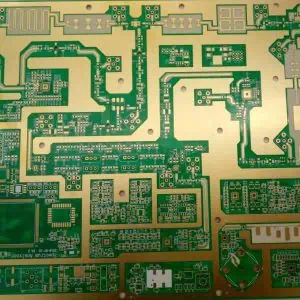
Trace design plays a crucial role in reliability. Wide traces reduce resistance and heat generation, while maintaining appropriate spacing prevents crosstalk and reduces the likelihood of electrical shorts. Designers should avoid sharp angles in trace routing, instead using curved or 45-degree angles to minimize stress concentrations that can lead to copper cracking. Via placement requires careful attention, as excessive via density can weaken the board mechanically, while inadequate via coverage can create thermal bottlenecks.
Component placement strategy directly affects reliability outcomes. Heat-generating components should be distributed evenly across the board to prevent thermal hotspots, with adequate spacing for heat dissipation. Critical components require protection from mechanical stress points, while sensitive analog circuits need isolation from digital switching noise sources. Power distribution networks must be designed with sufficient copper area and multiple paths to ensure stable voltage delivery under varying load conditions.
Thermal management represents one of the most critical aspects of reliable PCB design. Elevated temperatures accelerate most failure mechanisms, making effective heat dissipation paramount. Thermal vias help conduct heat away from components to ground planes or heat sinks, while copper pours provide additional thermal mass. Strategic component placement keeps temperature-sensitive devices away from heat sources, and thermal simulation during design validation helps identify potential problem areas before manufacturing.
Material Selection and Quality
The choice of PCB materials significantly influences reliability outcomes. Standard FR-4 materials work well for many applications, but high-reliability designs may require specialized materials with enhanced thermal, mechanical, or electrical properties.
Substrate materials must match the application’s thermal expansion requirements. Coefficient of thermal expansion (CTE) mismatches between the PCB and mounted components create mechanical stress during temperature cycling, potentially leading to solder joint failures or component cracking. High-temperature applications may require polyimide or ceramic substrates that maintain dimensional stability across wider temperature ranges.
Copper quality and thickness affect both electrical performance and mechanical reliability. Higher copper weights provide better current-carrying capacity and thermal conductivity but increase manufacturing costs and board thickness. The copper foil type and surface roughness influence adhesion to the substrate material, with smoother surfaces generally providing better high-frequency performance but potentially reduced mechanical bonding.
Solder mask and surface finish selections impact long-term reliability. Quality solder masks protect copper traces from oxidation and provide insulation between conductors, while appropriate surface finishes ensure reliable solderability over extended storage periods. HASL (Hot Air Solder Leveling), ENIG (Electroless Nickel Immersion Gold), and OSP (Organic Solderability Preservative) each offer different advantages depending on the application requirements and assembly processes.
Manufacturing Process Controls

Consistent manufacturing processes are essential for reliable PCB production. Process variations can introduce defects that may not manifest as immediate failures but can reduce long-term reliability through accelerated aging mechanisms.
Drilling operations require precise control to maintain hole quality and dimensional accuracy. Dull drill bits can cause rough hole walls or delamination around via sites, creating potential failure points. Proper drill bit selection, feed rates, and spindle speeds help maintain hole quality throughout production runs. Debris removal and desmearing processes ensure clean hole walls for reliable plating adhesion.
Plating processes must be carefully controlled to achieve uniform copper thickness and adhesion. Bath chemistry, temperature, and current density all affect plating quality. Non-uniform plating can create weak points in conductors, while poor adhesion between plating layers can lead to delamination failures. Regular bath analysis and test coupon evaluation help maintain consistent plating quality.
Etching processes require precise timing and chemistry control to achieve accurate trace dimensions without undercutting or rough edges. Over-etching can narrow traces below design specifications, increasing resistance and reducing current-carrying capacity. Under-etching may leave copper residues that can cause shorts between adjacent conductors.
Lamination processes must achieve proper bonding between layers while maintaining dimensional stability. Incorrect temperature, pressure, or timing can result in delamination, void formation, or warpage that affects component mounting and long-term reliability. Prepreg selection and handling procedures significantly influence lamination quality.
Environmental Stress Testing
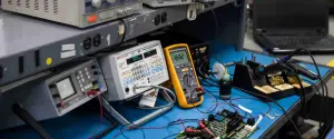
Comprehensive testing validates PCB reliability under expected operating conditions and helps identify potential failure modes before product deployment. Environmental stress testing should simulate the actual operating environment as closely as possible while accelerating aging mechanisms to predict long-term performance.
Thermal cycling tests subject PCBs to repeated temperature excursions that simulate power cycling or environmental temperature variations. These tests reveal solder joint fatigue, component lead fatigue, and thermal expansion-related failures. Test parameters should reflect actual operating conditions, including temperature ranges, ramp rates, and dwell times.
Humidity testing evaluates moisture resistance and helps identify potential corrosion or electrical leakage issues. High humidity environments can cause conductor corrosion, insulation resistance degradation, and electrochemical migration between conductors. Combined temperature and humidity testing provides more realistic stress conditions than either test alone.
Vibration and shock testing assess mechanical robustness under transportation and operational stresses. These tests can reveal weak solder joints, component mounting issues, or board flexure problems that might not appear under static conditions. Test frequencies and amplitudes should represent actual mechanical environments the product will encounter.
Quality Control and Inspection
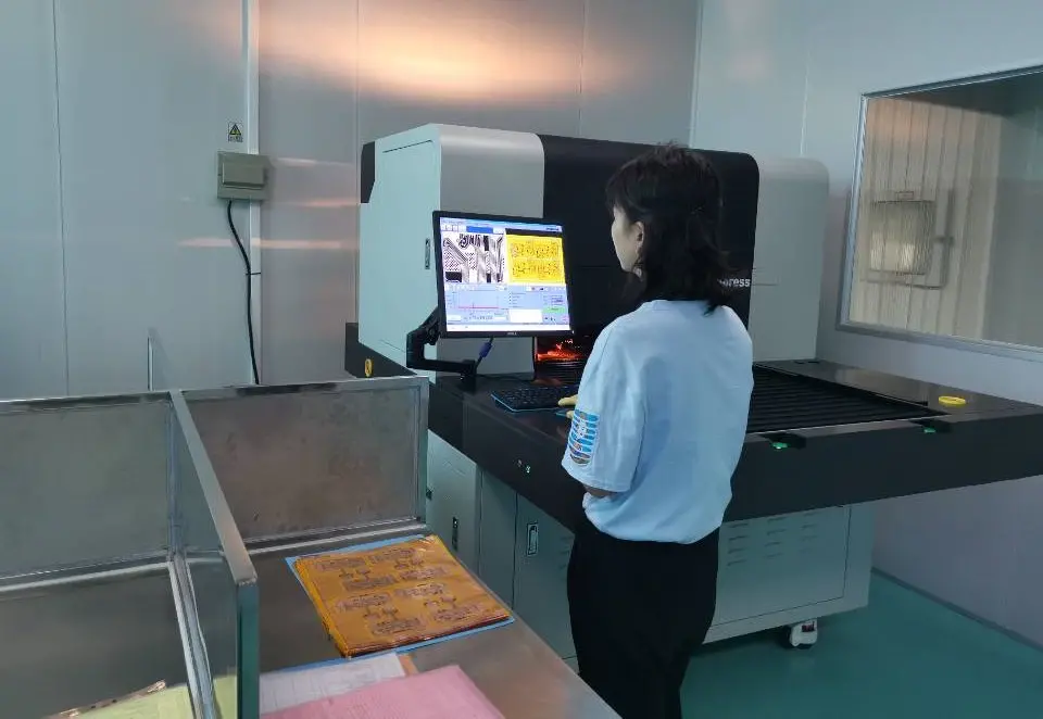
Rigorous quality control throughout the manufacturing process helps identify and eliminate defects before they reach customers. Multiple inspection points allow for early defect detection and process correction.
Automated optical inspection (AOI) systems can detect many surface defects including missing components, incorrect component placement, solder bridging, and insufficient solder joints. These systems provide consistent inspection capability and can identify defects that might be missed during manual inspection. However, AOI systems require proper programming and maintenance to remain effective.
In-circuit testing (ICT) verifies electrical connectivity and component values but may not detect all reliability-related issues. Flying probe testing offers flexibility for prototype and low-volume production but may not achieve the throughput required for high-volume manufacturing. Functional testing provides the most comprehensive verification but requires custom test fixtures and procedures.
X-ray inspection reveals hidden defects in ball grid array (BGA) components, through-hole solder joints, and internal via connections. This non-destructive testing method can identify voids, insufficient solder, and other defects that affect long-term reliability but may not cause immediate functional failures.
Design for Manufacturability and Reliability
Integrating manufacturability considerations into the design process improves both production yields and long-term reliability. Design rules that facilitate consistent manufacturing typically also enhance reliability by reducing process-induced stress and defects.
Component selection should consider not only electrical performance but also package reliability and supply chain stability. Packages with proven reliability records and established manufacturing processes typically exhibit fewer field failures than newer, less mature technologies. Standard component footprints and orientations simplify assembly processes and reduce the likelihood of placement errors.
Design rule compliance ensures compatibility with manufacturing capabilities while minimizing process-induced defects. Minimum trace widths, via sizes, and spacing requirements should align with manufacturing capabilities while providing adequate margins for process variations. Consistent design practices across multiple projects facilitate manufacturing learning and process optimization.
Documentation quality directly impacts manufacturing consistency and reliability outcomes. Clear assembly drawings, comprehensive bill of materials, and detailed fabrication specifications help ensure that manufacturing processes align with design intent. Regular communication between design and manufacturing teams helps identify potential issues early in the development process.
The pursuit of PCB reliability requires a comprehensive approach that encompasses design methodology, material selection, manufacturing process control, and validation testing. Success depends on understanding failure mechanisms, implementing appropriate preventive measures, and maintaining rigorous quality standards throughout the entire product development and manufacturing lifecycle. By following these principles and continuously improving processes based on field experience and advancing technology, engineers can achieve the high reliability levels demanded by today’s sophisticated electronic systems.