Silkscreen printing is a crucial process in the manufacturing of printed circuit boards (PCBs). It provides essential information and markings on the board surface, aiding in assembly, maintenance, and identification. This article will explore six key aspects of silkscreen printing for PCBs that every electronics engineer and PCB designer should know.
1. The Basics of Silkscreen Printing
What is Silkscreen Printing?
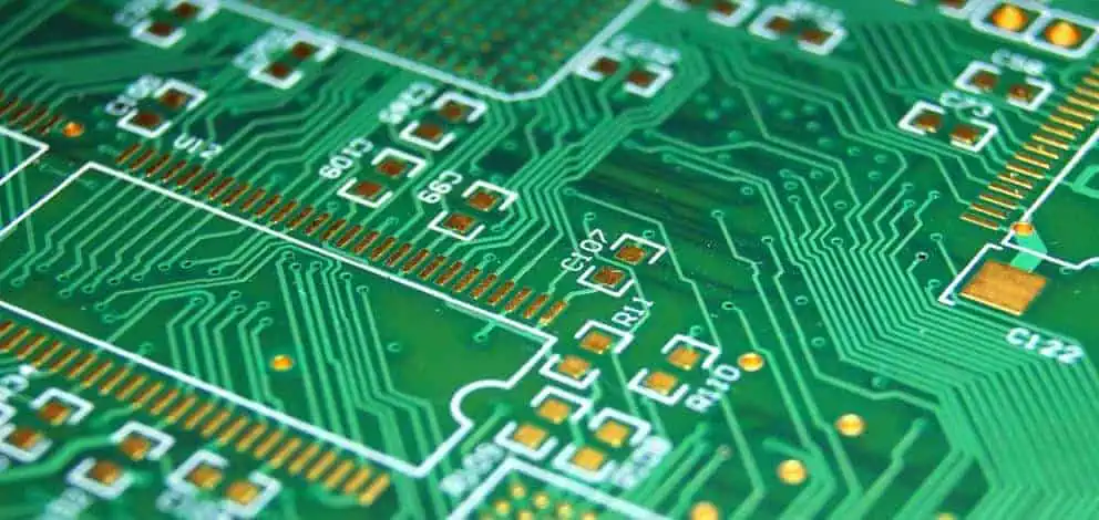
Silkscreen printing, also known as screen printing or silk screening, is a method of applying text, symbols, and other markings to the surface of a PCB. This process involves pushing ink through a fine mesh or screen onto the board, creating a thin layer of text or graphics.
The Purpose of Silkscreen on PCBs
The silkscreen layer serves several important functions:
- Component identification and orientation
- Pin numbering and labeling
- Board identification and branding
- Warning symbols and regulatory markings
- Assembly and testing instructions
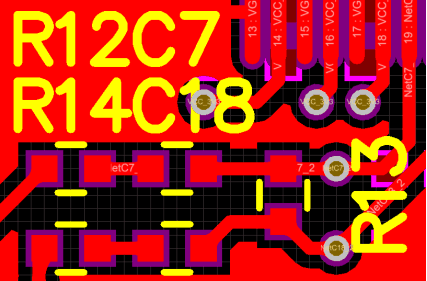
Common Silkscreen Colors

While white is the most common color for silkscreen printing on PCBs, other colors are also used for specific purposes or aesthetic reasons. Here’s a table showing common silkscreen colors and their typical uses:
| Color | Common Uses |
| White | Standard color for most PCBs |
| Yellow | High contrast on dark boards, caution indicators |
| Black | Used on light-colored boards (e.g., aluminum PCBs) |
| Red | Warnings, critical components, or aesthetic purposes |
| Green | Environmental or safety indications |
| Blue | Functional grouping or aesthetic purposes |
2. The Silkscreen Printing Process
Steps in Silkscreen Printing
The silkscreen printing process for PCBs typically involves the following steps:
- Design preparation
- Screen creation
- Board preparation
- Ink application
- Curing
- Quality control
Ink Types and Properties
The choice of ink is crucial for achieving high-quality, durable silkscreen prints. Here are some common ink types used in PCB silkscreen printing:
- Epoxy-based inks
- UV-curable inks
- Thermal-curable inks
- Solvent-based inks
Each ink type has its own properties, affecting factors such as durability, curing time, and environmental resistance.
Equipment Used in Silkscreen Printing
Silkscreen printing requires specialized equipment to ensure precise and consistent results. Key equipment includes:
- Screen printing machine
- Screens or stencils
- Squeegees
- Curing ovens or UV lamps
- Inspection systems
3. Design Considerations for Silkscreen Printing
Minimum Feature Size and Spacing
When designing the silkscreen layer, it’s essential to consider the minimum feature size and spacing that can be reliably printed. These limitations depend on various factors, including the printing equipment, ink properties, and board surface.
Here’s a table showing typical minimum feature sizes for silkscreen printing:
| Feature | Minimum Size |
| Text height | 0.032″ (0.8mm) |
| Line width | 0.006″ (0.15mm) |
| Space between lines | 0.006″ (0.15mm) |
| Filled areas | 0.020″ (0.5mm) |
Font Selection and Readability
Choosing the right font for silkscreen printing is crucial for ensuring readability and preventing smudging or bleeding. Some guidelines for font selection include:
- Use sans-serif fonts for better legibility
- Avoid fonts with fine details or thin strokes
- Consider using vector fonts for scalability
- Test readability at different sizes
Placement and Orientation
Proper placement and orientation of silkscreen elements are essential for effective communication and assembly. Consider the following:
- Align text and symbols with component orientation
- Avoid placing silkscreen on pads or vias
- Leave adequate space around components for easy reading
- Use consistent orientation for similar components
4. Common Challenges in Silkscreen Printing
Registration and Alignment Issues
Accurate registration and alignment of the silkscreen layer with the PCB features are critical for proper component identification and assembly. Common challenges include:
- Misalignment between silkscreen and component positions
- Shifting or stretching of the silkscreen during printing
- Inconsistent registration across multiple boards
Ink Adhesion and Durability
Ensuring proper ink adhesion and durability is essential for long-lasting silkscreen markings. Challenges in this area include:
- Poor adhesion to certain board materials or surface finishes
- Ink chipping or flaking during handling or assembly
- Fading or degradation due to environmental factors
Fine Detail Reproduction
Reproducing fine details in silkscreen printing can be challenging, especially for complex designs or small text. Issues to consider include:
- Bleeding or smudging of fine lines and small text
- Loss of detail in intricate symbols or logos
- Inconsistent ink coverage in small filled areas
5. Quality Control and Testing
Visual Inspection
Visual inspection is a crucial step in ensuring the quality of silkscreen printing. Key aspects to check include:
- Text legibility and clarity
- Alignment with board features and components
- Consistency of ink coverage
- Absence of smudges, bleeding, or other defects
Automated Optical Inspection (AOI)
AOI systems can be used to automate the inspection process for silkscreen printing. These systems can detect:
- Missing or misaligned silkscreen elements
- Incorrect text or symbols
- Defects in ink coverage or quality
Adherence and Durability Testing
To ensure the longevity of silkscreen markings, various tests can be performed:
- Tape test for adhesion
- Solvent resistance test
- Abrasion resistance test
- Thermal cycling test
Here’s a table summarizing common quality control tests for silkscreen printing:
| Test Type | Purpose | Method |
| Visual Inspection | Detect visible defects | Manual or automated visual examination |
| AOI | Identify errors and inconsistencies | Automated image analysis |
| Tape Test | Evaluate ink adhesion | Apply and remove adhesive tape |
| Solvent Resistance | Check chemical resistance | Expose to solvents used in manufacturing |
| Abrasion Test | Assess wear resistance | Mechanical abrasion with specified force |
| Thermal Cycling | Evaluate temperature stability | Expose to temperature extremes |
6. Advancements and Future Trends in Silkscreen Printing
Digital Printing Technologies
Advancements in digital printing technologies are beginning to impact PCB silkscreen printing. These include:
- Inkjet printing for PCB legend
- Direct imaging systems
- LED-UV curing technologies
Environmentally Friendly Inks and Processes
The industry is moving towards more environmentally friendly silkscreen printing options:
- Water-based inks
- Low-VOC (Volatile Organic Compound) formulations
- Energy-efficient curing systems
Integration with Other PCB Manufacturing Processes
Future trends in silkscreen printing include better integration with other PCB manufacturing processes:
- Inline printing and inspection systems
- Automated legend design based on PCB data
- Customizable and variable data printing
Frequently Asked Questions (FAQ)
Q1: What is the difference between silkscreen and solder mask on a PCB?
A1: While both silkscreen and solder mask are applied to the surface of a PCB, they serve different purposes. Silkscreen is used for printing text, symbols, and other markings to aid in assembly and identification. Solder mask is a thin lacquer-like layer of polymer that is applied to the copper traces of a PCB to prevent oxidation and to control where solder adheres during the soldering process.
Q2: Can silkscreen be applied on both sides of a PCB?
A2: Yes, silkscreen can be applied to both the top and bottom sides of a PCB. This is common in double-sided and multilayer PCBs where components or important information need to be identified on both sides of the board.
Q3: How durable is PCB silkscreen printing?
A3: The durability of PCB silkscreen printing depends on several factors, including the type of ink used, the curing process, and the environmental conditions the PCB is exposed to. High-quality silkscreen printing using epoxy or UV-curable inks can be very durable, resisting solvents, abrasion, and temperature changes. However, excessive handling or exposure to harsh chemicals can degrade the silkscreen over time.
Q4: Can silkscreen be removed or changed after PCB manufacturing?
A4: While it is possible to remove or change silkscreen after PCB manufacturing, it is not recommended and can be challenging. Removing silkscreen typically involves using solvents or mechanical abrasion, which can damage the underlying solder mask or copper layers. Adding new silkscreen markings after manufacturing is possible but may not adhere as well as the original printing. It’s always best to ensure the silkscreen design is correct before manufacturing.
Q5: How does silkscreen printing affect the overall cost of PCB production?
A5: Silkscreen printing is generally considered a standard part of PCB production and doesn’t significantly impact the overall cost. However, certain factors can increase costs:
- Use of non-standard colors
- Very complex or high-resolution designs
- Two-sided silkscreen printing
- Special inks for specific requirements (e.g., high temperature resistance)
The cost impact is usually minimal compared to other aspects of PCB production, and the benefits of clear component identification and assembly instructions often outweigh any additional expenses.