The Printed Circuit Board (PCB) industry is constantly evolving, with new technologies and processes emerging to meet the demands of modern electronics. One such innovation is the PCB embedded component process, a technique that has gained significant attention in recent years. This article will delve into the intricacies of this process, exploring its benefits, challenges, and applications in various industries.
Understanding PCB Embedded Components
Definition and Concept
PCB embedded component process, also known as component embedding or embedded passive and active (EP&A) technology, refers to the practice of integrating electronic components directly into the layers of a printed circuit board during the manufacturing process. This technique differs from traditional surface-mount technology (SMT) or through-hole mounting, as components are literally embedded within the PCB structure itself.
Types of Embedded Components
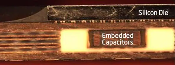
Several types of components can be embedded in PCBs:
- Passive components
- Resistors
- Capacitors
- Inductors
- Active components
- Integrated circuits (ICs)
- Semiconductors
- Other elements
- Antennas
- Sensors
The PCB Embedded Component Process
Step-by-Step Breakdown
The process of embedding components into PCBs involves several key steps:
- Design and planning
- Component preparation
- Cavity creation
- Component placement
- Lamination
- Via drilling and plating
- Outer layer circuitry
- Final testing and inspection
Let’s explore each of these steps in more detail.
1. Design and Planning
The embedded component process begins with careful design and planning. Engineers must consider factors such as:
- Component selection
- Optimal placement within PCB layers
- Thermal management
- Signal integrity
- Manufacturing feasibility
Advanced PCB design software is typically used to create detailed layouts and simulations.
2. Component Preparation
Components intended for embedding often require special preparation:
- Passive components may be supplied in sheet form
- Active components might need thinning or special packaging
- Some components may require additional protective coatings
3. Cavity Creation
Cavities are created in the PCB layers to accommodate the embedded components:
- Laser ablation or mechanical milling techniques are commonly used
- Precision is crucial to ensure proper fit and alignment
4. Component Placement
Components are carefully placed into the prepared cavities:
- Automated pick-and-place machines or manual placement may be used
- Alignment and orientation must be precise
5. Lamination
Once components are in place, additional PCB layers are laminated over them:
- Heat and pressure are applied to bond the layers
- Special care is taken to avoid damaging the embedded components
6. Via Drilling and Plating
Vias are drilled to create electrical connections:
- Laser or mechanical drilling techniques are employed
- Vias are plated to establish conductivity between layers
7. Outer Layer Circuitry
The outer layers of the PCB are processed:
- Copper patterns are etched or plated
- Additional surface-mount or through-hole components may be added
8. Final Testing and Inspection
Rigorous testing ensures the functionality and reliability of the embedded components:
- Electrical testing
- X-ray inspection
- Thermal imaging
Advantages of PCB Embedded Component Process
The embedded component process offers several significant advantages:
1. Miniaturization
By integrating components within the PCB layers, designers can achieve:
- Reduced overall PCB size
- Higher component density
- More compact electronic devices
2. Improved Performance
Embedded components can lead to enhanced electrical performance:
- Shorter signal paths
- Reduced parasitic effects
- Better signal integrity
3. Enhanced Reliability
The embedded nature of components provides protection:
- Reduced exposure to environmental factors
- Lower risk of mechanical stress
- Improved thermal management
4. Cost Efficiency
While initial costs may be higher, embedded components can offer long-term savings:
- Reduced assembly steps
- Fewer external components needed
- Potential for automation in manufacturing
5. Design Flexibility
Embedding components allows for greater design freedom:
- Multi-functional PCB layers
- Optimization of space utilization
- Ability to create unique form factors
Challenges and Limitations
Despite its advantages, the PCB embedded component process faces several challenges:
1. Manufacturing Complexity
Embedding components requires specialized equipment and expertise:
- Higher initial investment in manufacturing capabilities
- More complex production processes
- Increased potential for errors during manufacturing
2. Thermal Management
Heat dissipation can be more challenging with embedded components:
- Limited access to components for cooling
- Potential for hot spots within the PCB
3. Repairability and Rework
Embedded components are difficult or impossible to replace:
- Limited options for repair
- Entire PCB may need replacement in case of component failure
4. Testing and Quality Control
Inspecting and testing embedded components presents unique challenges:
- Limited visual inspection possibilities
- Need for advanced testing equipment (e.g., X-ray systems)
5. Cost Considerations
While there are potential long-term savings, initial costs can be higher:
- Specialized manufacturing equipment required
- Potentially lower yields, especially during initial implementation
Applications of PCB Embedded Component Process
The embedded component technology finds applications in various industries:
1. Consumer Electronics
- Smartphones
- Wearable devices
- Tablets and laptops
2. Automotive Industry
- Advanced driver assistance systems (ADAS)
- Electric vehicle control units
- Infotainment systems
3. Aerospace and Defense
- Avionics systems
- Satellite communications
- Radar and electronic warfare equipment
4. Medical Devices
- Implantable medical devices
- Portable diagnostic equipment
- Hearing aids
5. Industrial Applications
- IoT sensors and devices
- Industrial control systems
- Robotics
Future Trends and Developments
The PCB embedded component process continues to evolve:
1. Advanced Materials
Research into new materials for both PCBs and components:
- High-frequency substrates
- Thermally conductive materials
- Flexible and stretchable substrates
2. 3D Printing Integration
Exploration of 3D printing technologies for PCB fabrication:
- Potential for customized embedded components
- Rapid prototyping capabilities
3. Artificial Intelligence and Machine Learning
AI and ML applications in design and manufacturing:
- Optimized component placement
- Predictive maintenance for manufacturing equipment
- Enhanced quality control processes
4. Increased Automation
Further automation of the embedding process:
- Improved precision and repeatability
- Reduced manufacturing costs
- Higher production volumes
5. Sustainability Efforts
Focus on environmentally friendly practices:
- Development of recyclable PCB materials
- Reduction of waste in the manufacturing process
- Energy-efficient production methods
Comparison: Traditional PCB vs. Embedded Component PCB
To better understand the differences between traditional PCB assembly and the embedded component process, let’s compare key aspects:
| Aspect | Traditional PCB | Embedded Component PCB |
| Component Placement | Surface-mount or through-hole | Within PCB layers |
| Board Size | Larger due to surface components | Compact due to embedded components |
| Signal Path Length | Longer | Shorter |
| Electromagnetic Interference | More susceptible | Reduced interference |
| Thermal Management | Easier access for cooling | More challenging, requires careful design |
| Manufacturing Complexity | Lower | Higher |
| Initial Cost | Lower | Higher |
| Long-term Cost | Potentially higher | Potentially lower |
| Repairability | Easier to repair/replace components | Difficult or impossible to repair |
| Design Flexibility | Limited by surface area | Greater 3D design possibilities |
Frequently Asked Questions (FAQ)
1. What is the main difference between embedded components and surface-mount components?
Embedded components are integrated within the layers of the PCB during manufacturing, while surface-mount components are placed on the outer surfaces of the PCB after the board is fabricated. This key difference allows embedded components to create more compact designs with potentially better electrical performance.
2. Are all types of electronic components suitable for embedding in PCBs?
Not all components are suitable for embedding. Generally, passive components like resistors and capacitors are most commonly embedded. Some active components, such as certain ICs and semiconductors, can also be embedded if they meet specific size and packaging requirements. However, larger or more complex components may not be suitable for embedding due to size constraints or thermal management issues.
3. How does the PCB embedded component process affect the overall cost of manufacturing?
The embedded component process typically involves higher initial costs due to the need for specialized equipment and more complex manufacturing processes. However, it can lead to long-term cost savings through reduced assembly steps, fewer external components, and the potential for creating more compact devices. The cost-effectiveness often depends on the production volume and specific application requirements.
4. What are the main challenges in repairing or reworking PCBs with embedded components?
Repairing or reworking PCBs with embedded components is significantly more challenging than traditional PCBs. The main difficulties include:
- Limited access to embedded components
- Risk of damaging surrounding PCB layers during repair attempts
- Inability to visually inspect embedded components
- Lack of standardized repair procedures for embedded components
In many cases, if an embedded component fails, the entire PCB may need to be replaced rather than repaired.
5. How does the embedded component process impact the thermal management of a PCB?
Thermal management can be more complex with embedded components. While embedding can sometimes improve heat dissipation by allowing components to transfer heat directly to inner PCB layers, it can also create challenges:
- Limited access to components for external cooling solutions
- Potential for heat buildup within PCB layers
- Need for careful thermal design and material selection
Designers must consider thermal management early in the design process, often using thermal simulation tools to optimize heat dissipation in embedded component PCBs.