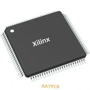
The XC7K70T-1FBG676C is a powerful field-programmable gate array (FPGA) from Xilinx’s Kintex-7 family, designed to deliver exceptional performance for demanding digital signal processing, communications, and embedded processing applications. This advanced FPGA combines high logic density with energy-efficient architecture, making it an ideal choice for engineers developing next-generation electronic systems.
Product Specifications
The XC7K70T-1FBG676C features robust specifications that make it suitable for complex digital designs. This FPGA incorporates 65,600 logic cells and 4,860 configurable logic blocks (CLBs), providing ample resources for sophisticated applications. The device includes 6,270 slices, each containing four 6-input lookup tables (LUTs) and eight flip-flops, enabling flexible logic implementation.
Memory capabilities of the XC7K70T-1FBG676C include 270 block RAM tiles totaling 4.86 Mb of internal memory, plus 1,040 Kb of distributed RAM. The FPGA supports up to 300 user I/O pins in the FBGA676 package, facilitating extensive connectivity options for system integration.
The device operates with DSP capabilities through 240 DSP48E1 slices, optimized for high-performance signal processing applications. The XC7K70T-1FBG676C supports clock management through four mixed-mode clock managers (MMCMs) and four phase-locked loops (PLLs), ensuring precise timing control across the design.
This FPGA utilizes 28nm technology and operates across commercial temperature ranges from 0°C to +85°C. The device supports multiple I/O standards including LVCMOS, LVDS, and differential signaling, providing versatility for various interface requirements.
Price Information
Pricing for the XC7K70T-1FBG676C varies based on quantity, supplier, and current market conditions. The device typically falls within the mid-range pricing tier of Kintex-7 FPGAs, reflecting its balanced performance and resource allocation. Volume pricing discounts are generally available for production quantities, making the XC7K70T-1FBG676C cost-effective for commercial applications.
For current pricing information, engineers should contact authorized Xilinx distributors or check electronic component marketplaces. Educational pricing may be available for academic institutions and students working on research projects involving the XC7K70T-1FBG676C.
Documents & Media
Comprehensive documentation supports the XC7K70T-1FBG676C throughout the design process. The primary datasheet provides detailed electrical specifications, timing characteristics, and package information essential for system design. Pin configuration diagrams and package drawings facilitate accurate PCB layout and routing.
Programming and configuration guides explain the various methods for loading designs into the XC7K70T-1FBG676C, including JTAG, SelectMAP, and serial configuration options. Application notes cover specific implementation topics such as power management, signal integrity, and thermal considerations.
Design methodology guides help engineers optimize their HDL code for the XC7K70T-1FBG676C architecture. Reference designs and example projects demonstrate best practices for common applications including digital signal processing, communication interfaces, and embedded processing systems.
Video tutorials and webinars provide visual learning resources for engineers new to FPGA development or the Kintex-7 family. These materials complement written documentation and accelerate the learning curve for the XC7K70T-1FBG676C.
Related Resources
Development tools for the XC7K70T-1FBG676C include Xilinx Vivado Design Suite, which provides synthesis, implementation, and debugging capabilities. The software supports both schematic and HDL-based design entry, accommodating different engineering preferences and project requirements.
Evaluation boards featuring the XC7K70T-1FBG676C enable rapid prototyping and proof-of-concept development. These boards typically include essential peripherals, connectors, and reference designs that accelerate project timelines.
IP cores compatible with the XC7K70T-1FBG676C expand functionality without requiring custom development. Available IP includes communication protocols, memory controllers, and mathematical functions optimized for the Kintex-7 architecture.
Training courses and certification programs help engineers develop expertise with the XC7K70T-1FBG676C and FPGA design methodologies. Online and classroom options accommodate different learning preferences and schedules.
Third-party tools and libraries extend the development ecosystem for the XC7K70T-1FBG676C. These resources include simulation tools, verification environments, and specialized design flows for specific application domains.
Environmental & Export Classifications
The XC7K70T-1FBG676C meets RoHS compliance standards, ensuring environmentally responsible manufacturing and disposal practices. The device is halogen-free and uses lead-free assembly processes, supporting green electronics initiatives.
Operating temperature specifications for the XC7K70T-1FBG676C cover commercial grade requirements from 0°C to +85°C. The device is designed for reliable operation across this temperature range while maintaining specified performance characteristics.
Export control classifications for the XC7K70T-1FBG676C follow applicable regulations for electronic components. Engineers should verify current export requirements when planning international shipments or projects involving the device.
The FBGA676 package of the XC7K70T-1FBG676C uses industry-standard materials and assembly techniques, ensuring compatibility with standard PCB manufacturing processes. Package moisture sensitivity level and storage requirements are specified to maintain device reliability.
Power consumption characteristics of the XC7K70T-1FBG676C support energy-efficient system designs. Static and dynamic power specifications help engineers optimize their power budgets and thermal management strategies for applications using this FPGA.
The XC7K70T-1FBG676C represents an excellent balance of performance, resources, and cost-effectiveness for advanced FPGA applications. Its comprehensive feature set and extensive support ecosystem make it a reliable choice for engineers developing innovative electronic systems across multiple industries.


