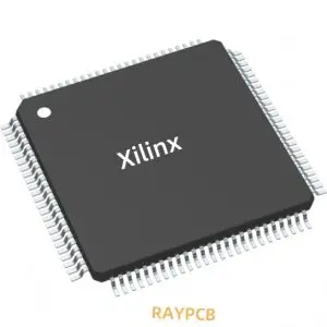
The XC7K410T-3FFG900C represents a cutting-edge Field-Programmable Gate Array (FPGA) from Xilinx’s renowned Kintex-7 family, delivering exceptional performance for demanding applications in telecommunications, aerospace, defense, and industrial automation. This advanced programmable logic device combines high-speed processing capabilities with energy efficiency, making it an ideal choice for complex digital signal processing and high-bandwidth applications.
Product Specifications
The XC7K410T-3FFG900C features impressive technical specifications that set it apart in the FPGA market. This device incorporates 406,720 logic cells and 28,620 Configurable Logic Blocks (CLBs), providing extensive programmable resources for complex designs. The FPGA includes 1,540 DSP48E1 slices, enabling high-performance digital signal processing operations essential for communications and multimedia applications.
Memory resources are abundant with 28,620 Kbit of block RAM and 38,400 distributed RAM bits, ensuring adequate storage for data-intensive applications. The XC7K410T-3FFG900C supports up to 500 user I/O pins, facilitating extensive connectivity options for system integration. The device operates at a -3 speed grade, delivering superior timing performance for high-frequency applications.
Built on advanced 28nm technology, the XC7K410T-3FFG900C offers reduced power consumption while maintaining high performance. The FFG900 package provides a compact 31mm x 31mm footprint with a 0.8mm ball pitch, optimizing board space utilization. The device supports multiple I/O standards including LVDS, DDR3, and PCIe, ensuring compatibility with various system interfaces.
Price Information
Pricing for the XC7K410T-3FFG900C varies based on order quantity, distribution channel, and current market conditions. For accurate pricing information and volume discounts, customers should contact authorized Xilinx distributors or visit official pricing portals. The investment in this high-performance FPGA delivers significant value through its versatile capabilities and long-term support from Xilinx.
Documents & Media
Comprehensive technical documentation supports the XC7K410T-3FFG900C implementation process. The official datasheet provides detailed electrical specifications, timing parameters, and package information essential for design engineers. Pin-out diagrams and package drawings facilitate accurate PCB layout and routing decisions.
Application notes cover specific implementation guidance for common use cases, while reference designs demonstrate best practices for leveraging the device’s capabilities. The Xilinx development environment includes extensive documentation on design flows, constraint files, and optimization techniques specific to the XC7K410T-3FFG900C.
Video tutorials and webinars offer visual learning resources for engineers new to Kintex-7 FPGAs. Technical support forums provide community-driven assistance and real-world implementation insights from experienced developers working with the XC7K410T-3FFG900C.
Related Resources
The XC7K410T-3FFG900C ecosystem includes powerful development tools and complementary products. Xilinx Vivado Design Suite provides the primary development environment, offering synthesis, implementation, and debugging capabilities optimized for Kintex-7 devices. ChipScope Pro and Vivado Logic Analyzer enable real-time debugging and signal analysis.
Evaluation boards and development kits accelerate prototype development and proof-of-concept implementations. These platforms provide pre-configured hardware environments for testing XC7K410T-3FFG900C functionality without custom PCB development. Reference designs for common applications like video processing, communications, and motor control demonstrate practical implementation approaches.
Third-party IP cores extend the XC7K410T-3FFG900C capabilities, offering pre-verified solutions for complex functions like encryption, compression, and protocol processing. Training courses and certification programs help engineers maximize their proficiency with Kintex-7 FPGA development.
Environmental & Export Classifications
The XC7K410T-3FFG900C meets stringent environmental and regulatory standards for commercial and industrial applications. The device operates reliably across a junction temperature range of 0°C to +85°C, suitable for most commercial environments. Extended temperature variants support industrial applications requiring operation in harsh conditions.
RoHS compliance ensures the XC7K410T-3FFG900C meets European environmental standards for hazardous substance restrictions. The device carries appropriate export control classifications, with specific requirements varying by destination country and end-use application. Customers must verify export compliance requirements for their specific applications and geographic markets.
Quality certifications include ISO 9001 manufacturing standards and automotive-grade options for safety-critical applications. The XC7K410T-3FFG900C undergoes rigorous testing and validation processes to ensure consistent performance and reliability across production batches.
Environmental testing covers thermal cycling, humidity exposure, and mechanical stress conditions typical in real-world applications. These comprehensive validation procedures ensure the XC7K410T-3FFG900C delivers dependable operation throughout its operational lifetime, making it a trusted choice for mission-critical applications requiring proven FPGA performance.


