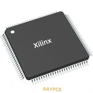
The XC2S100-5TQG144I is a high-performance field-programmable gate array (FPGA) from Xilinx’s Spartan-II family, designed for cost-effective digital signal processing and general-purpose logic applications. This versatile FPGA delivers exceptional performance in a compact 144-pin TQFP package, making it ideal for space-constrained designs requiring reliable programmable logic solutions.
Product Specifications
The XC2S100-5TQG144I features robust technical specifications that make it suitable for diverse embedded applications. This FPGA contains 100,000 system gates with 2,500 logic cells, providing ample resources for complex digital designs. The device operates at a -5 speed grade, ensuring fast signal processing capabilities with maximum operating frequencies up to 200 MHz.
Key technical specifications of the XC2S100-5TQG144I include 4,000 equivalent logic gates, 40 Kbits of block RAM, and 176 user I/O pins. The device supports 3.3V core voltage operation with 5V-tolerant I/O, enabling seamless integration with both modern and legacy systems. The industrial temperature range (-40°C to +85°C) ensures reliable operation in harsh environmental conditions.
The XC2S100-5TQG144I utilizes advanced SRAM-based configuration technology, allowing for infinite reprogrammability during development and field updates. This flexibility makes it an excellent choice for prototyping, low-volume production, and applications requiring field upgrades.
Price Information
Pricing for the XC2S100-5TQG144I varies based on quantity, supplier, and market conditions. Industrial and commercial buyers typically find competitive pricing through authorized Xilinx distributors and electronic component suppliers. Volume pricing discounts are generally available for quantities exceeding 100 units, with additional savings for annual purchase agreements.
For current XC2S100-5TQG144I pricing information, contact authorized distributors such as Digi-Key, Mouser Electronics, Arrow Electronics, or Avnet. Many suppliers offer online pricing calculators that provide real-time quotes based on quantity requirements and delivery schedules.
Documents & Media
Comprehensive documentation supports XC2S100-5TQG144I implementation and design optimization. Essential documents include the official datasheet detailing electrical characteristics, timing specifications, and package information. The Spartan-II FPGA Family User Guide provides detailed architectural information and design guidelines specific to the XC2S100-5TQG144I.
Application notes covering clock management, I/O standards, and power optimization techniques help engineers maximize XC2S100-5TQG144I performance. Design files including IBIS models, package drawings, and pin assignment files are available through Xilinx’s official website and design tools.
The Xilinx ISE Design Suite provides complete development environment support for the XC2S100-5TQG144I, including synthesis, place-and-route, and timing analysis tools. Reference designs and example projects demonstrate practical implementation techniques for common applications.
Related Resources
Engineers working with the XC2S100-5TQG144I benefit from extensive ecosystem support and related products. Development boards featuring the XC2S100-5TQG144I provide hands-on evaluation platforms for rapid prototyping and proof-of-concept development. These boards typically include essential peripherals, power supplies, and programming interfaces.
Compatible configuration devices such as XC18V00 series PROMs enable standalone operation of XC2S100-5TQG144I systems. Clock management solutions including dedicated clock buffers and crystal oscillators optimize timing performance in XC2S100-5TQG144I designs.
The broader Spartan-II family offers migration paths for scaling applications, with pin-compatible devices ranging from XC2S50 to XC2S200. This compatibility enables easy design migration when requirements change or cost optimization is needed.
Environmental & Export Classifications
The XC2S100-5TQG144I meets stringent environmental and regulatory standards for industrial applications. RoHS compliance ensures lead-free manufacturing processes, while REACH regulation compliance confirms restricted substance management. The device carries appropriate CE marking for European market acceptance.
Export classification information indicates the XC2S100-5TQG144I falls under standard commercial export categories, typically requiring minimal export licensing for most destinations. However, specific applications in sensitive industries or restricted countries may require additional export compliance review.
Environmental operating specifications include extended temperature range capability (-40°C to +85°C junction temperature) and resistance to vibration, shock, and humidity as defined in relevant JEDEC standards. The XC2S100-5TQG144I package construction ensures long-term reliability in demanding industrial environments.
Quality certifications include ISO 9001 manufacturing standards and automotive-grade quality processes where applicable. These certifications support XC2S100-5TQG144I deployment in critical applications requiring proven reliability and consistent performance.
The XC2S100-5TQG144I represents proven FPGA technology combining performance, flexibility, and cost-effectiveness for modern digital designs. Its comprehensive feature set and robust support ecosystem make it an excellent choice for engineers developing innovative programmable logic solutions.


