A 4-layer PCB stackup is one of the most common multilayer board configurations used in modern electronics, offering an excellent balance between functionality, cost, and manufacturability. This stackup consists of four conductive copper layers separated by three dielectric layers, providing designers with enhanced routing capabilities while maintaining controlled impedance and good signal integrity.
Standard 4-Layer Configuration
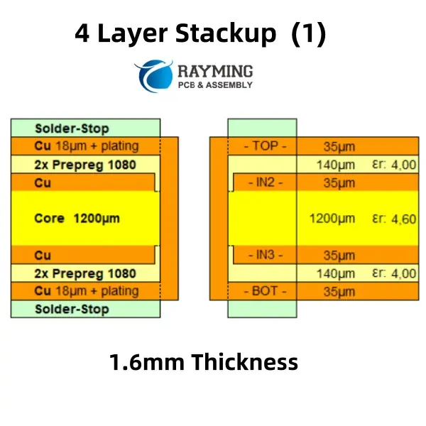
The typical 4-layer stackup follows a symmetric arrangement: Signal-Ground-Power-Signal, often abbreviated as Sig-Gnd-Pwr-Sig. The top layer (Layer 1) serves as the primary component and signal routing layer, while the bottom layer (Layer 4) provides additional signal routing and component placement. The two internal layers (Layers 2 and 3) are dedicated to ground and power planes respectively, creating a solid reference structure for the outer signal layers.
Layer Functions and Characteristics
Layer 1 (Top Signal) typically handles high-speed digital signals, analog circuits, and surface-mount component connections. This layer offers the most flexibility for routing and component placement. Layer 2 (Ground Plane) provides a continuous ground reference, acting as a return path for signals and offering electromagnetic shielding. Layer 3 (Power Plane) distributes power throughout the board, often split into multiple voltage domains as needed. Layer 4 (Bottom Signal) accommodates additional routing, often for lower-speed signals, and provides space for through-hole components and additional surface-mount devices.
Dielectric and Thickness Considerations
The dielectric material between layers, typically FR-4, determines the board’s electrical and mechanical properties. A common thickness distribution includes 0.1mm for outer copper layers and 0.035mm for inner layers, with dielectric thicknesses of approximately 0.2mm between Layer 1-2, 1.0mm between Layers 2-3 (core), and 0.2mm between Layers 3-4. This configuration results in a total board thickness of around 1.6mm, which is industry standard.
Impedance Control and Signal Integrity
The 4-layer stackup excels at impedance control due to the adjacent ground and power planes. Microstrip traces on the outer layers reference the nearest plane (typically ground), while stripline configurations can be created by routing between the power and ground planes. This arrangement minimizes crosstalk, reduces electromagnetic interference (EMI), and provides stable characteristic impedance for high-speed signals.
Design Advantages
This stackup offers several key benefits including improved power distribution through dedicated power planes, enhanced signal integrity via solid reference planes, reduced EMI through better shielding, and increased routing density compared to 2-layer boards. The symmetric structure also minimizes warpage during manufacturing and thermal cycling.
Manufacturing and Cost Considerations
4-layer boards represent a sweet spot in the cost-complexity curve. They’re significantly more affordable than 6+ layer boards while offering substantial improvements over 2-layer designs. Most PCB manufacturers have optimized processes for 4-layer production, ensuring good yield rates and competitive pricing.
Applications
This stackup is ideal for moderate-complexity digital designs, mixed-signal circuits, power supplies, communication devices, and consumer electronics where cost sensitivity exists but improved performance over 2-layer boards is required. It’s particularly well-suited for designs operating at frequencies up to several hundred MHz, making it perfect for microcontroller-based systems, IoT devices, and general-purpose electronic products.


