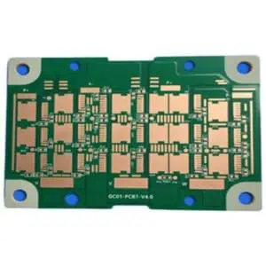
Product Overview
Skip Via PCB technology enables selective electrical connections between non-adjacent layers in multilayer printed circuit boards, allowing signals to bypass intermediate layers while maintaining signal integrity and optimizing routing efficiency.
Key Features
Selective Layer Routing: Connect specific layers while skipping intermediate layers, providing greater design flexibility and reducing signal path complexity.
Enhanced Signal Integrity: Minimizes crosstalk and electromagnetic interference by allowing direct connections between target layers without unnecessary layer transitions.
Space Optimization: Reduces the need for complex routing patterns and via farms, maximizing board real estate utilization.
High-Density Integration: Enables more compact PCB designs by eliminating redundant via structures and optimizing vertical interconnect architecture.
Controlled Impedance: Maintains consistent impedance characteristics across skipped layer connections, ensuring reliable high-speed signal transmission.
Technical Specifications
- Layer Count: Compatible with 4-32 layer PCB stackups
- Via Diameter: 0.1mm to 0.3mm (4-12 mils)
- Aspect Ratio: Up to 15:1 depending on board thickness
- Operating Frequency: DC to 40+ GHz
- Temperature Range: -55°C to +125°C
- Dielectric Materials: Compatible with FR-4, Rogers, and polyimide substrates
Applications
Perfect for high-speed digital designs, RF/microwave circuits, dense BGA routing, power distribution networks, and advanced packaging applications where traditional via structures create routing constraints or signal integrity challenges.
Manufacturing Requirements
Requires advanced drilling and plating processes with precise depth control. Compatible with standard PCB fabrication equipment with HDI (High Density Interconnect) capabilities.