Advanced Multi-Layer Circuit Board Manufacturing for High-Density Applications
Sequential lamination PCB technology represents the pinnacle of modern printed circuit board manufacturing, enabling the creation of ultra-high-density interconnect (HDI) boards with exceptional performance characteristics. This advanced build-up process constructs PCBs layer by layer through multiple lamination cycles, allowing for complex routing architectures and miniaturized designs that traditional manufacturing methods cannot achieve.
Key Features
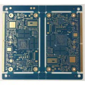
Multi-Stage Build-Up Process: Our sequential lamination technology builds PCBs through controlled, step-by-step layer addition, creating boards with 4 to 20+ layers while maintaining precise dimensional tolerances and electrical performance specifications.
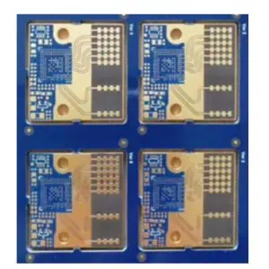
Micro-Via Integration: Incorporates laser-drilled micro-vias as small as 50μm diameter, enabling high-density interconnections between layers with minimal real estate consumption. These micro-vias can be stacked, staggered, or filled as required by your design specifications.
Fine Line/Space Capabilities: Achieves trace widths and spacing down to 25μm (1 mil), supporting the most demanding high-frequency and high-speed digital applications where signal integrity is paramount.
Mixed Via Architecture: Combines through-hole vias, blind vias, buried vias, and micro-vias within a single board structure, providing maximum routing flexibility for complex multi-layer designs.
Technical Specifications
- Layer Count: 4-30 layers with sequential build-up
- Minimum Via Size: 50μm laser-drilled micro-vias
- Trace Width/Spacing: Down to 25μm/25μm
- Board Thickness: 0.2mm to 6.0mm final thickness
- Via Aspect Ratio: Up to 12:1 for mechanical drilling, 1:1 for laser micro-vias
- Registration Accuracy: ±25μm between layers
- Impedance Control: ±5% tolerance for controlled impedance traces
Applications
Sequential lamination PCBs excel in applications requiring maximum functionality in minimal space. Primary markets include smartphones and mobile devices, high-performance computing systems, automotive electronics including ADAS and infotainment systems, medical devices requiring biocompatibility, aerospace and defense electronics, 5G infrastructure equipment, and IoT devices where size constraints are critical.
Manufacturing Advantages
The sequential build-up process provides superior design flexibility compared to conventional PCB manufacturing. Engineers can optimize layer stackups for specific electrical requirements, implement complex routing schemes impossible with traditional methods, and achieve higher component density through reduced via sizes and optimized layer utilization. The controlled lamination process ensures excellent layer-to-layer registration and consistent electrical performance across the entire board.
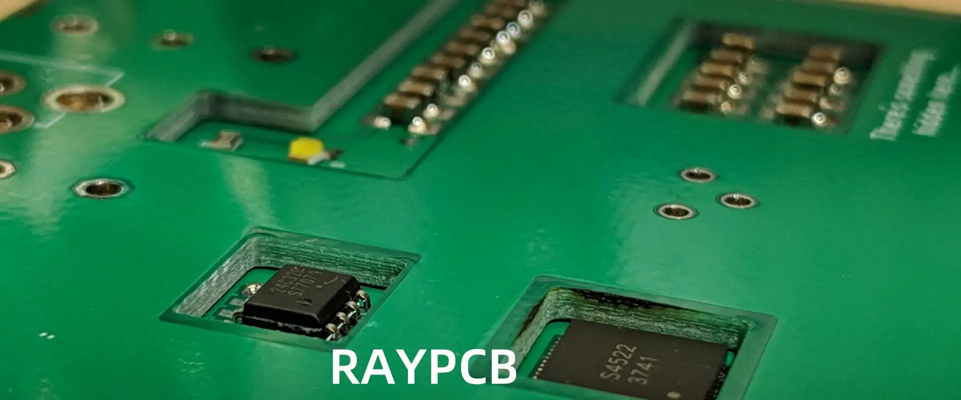
Quality Assurance: Each lamination cycle includes comprehensive testing and inspection protocols. Automated optical inspection (AOI), electrical testing, and microsectioning analysis ensure every board meets stringent quality standards before proceeding to the next build-up stage.
Sequential lamination PCB technology enables the next generation of electronic devices by providing the foundation for increasingly sophisticated circuit designs while maintaining the reliability and performance standards demanded by modern applications.