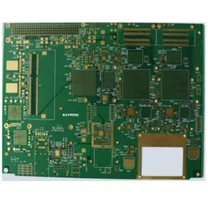
Sequential lamination PCBs represent the cutting-edge of high-density interconnect (HDI) manufacturing, enabling the creation of ultra-complex multilayer circuit boards through progressive build-up processes. This advanced technology allows manufacturers to construct PCBs layer by layer, adding conductive and insulating materials in precise sequences to achieve exceptional circuit density and performance.
Key Features & Capabilities:
Our sequential lamination process supports multiple build-up configurations, from simple 1+N+1 structures to complex any-layer HDI designs. The technology enables the integration of microvias, buried vias, and through-hole vias in sophisticated combinations, allowing for optimal signal routing in space-constrained applications. With layer counts ranging from 4 to 40+ layers, these PCBs can accommodate the most demanding electronic designs.
Advanced Manufacturing Process:
The sequential build-up process begins with a core substrate, followed by the systematic addition of prepreg layers, copper foil, and precise drilling of microvias using laser or mechanical methods. Each layer undergoes controlled lamination under specific temperature and pressure conditions, ensuring superior adhesion and dimensional stability. Advanced plating processes fill microvias and establish reliable interconnections between layers, while sophisticated surface treatments provide optimal solderability and durability.
Performance Benefits:
Sequential lamination technology delivers exceptional signal integrity through controlled impedance and reduced electromagnetic interference. The precise layer-to-layer registration achieves tolerances of ±25μm, while the optimized dielectric properties support high-frequency applications up to millimeter-wave frequencies. The robust construction provides excellent thermal management and mechanical reliability, with IPC Class 3 compliance for mission-critical applications.
Applications:
Ideal for telecommunications infrastructure, 5G equipment, advanced computing systems, automotive electronics, medical devices, and aerospace applications where miniaturization, performance, and reliability are paramount. The technology excels in applications requiring high pin-count BGAs, dense component placement, and complex routing requirements.
Quality Assurance:
Every sequential lamination PCB undergoes comprehensive testing including electrical continuity, insulation resistance, impedance control verification, and advanced inspection using automated optical inspection (AOI) and X-ray analysis to ensure defect-free manufacturing and consistent performance.