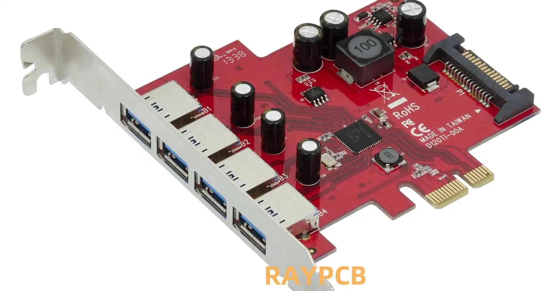
Precision-Engineered Testing Solutions for Advanced Research Applications
Our Research PCB Prototypes are specialized laboratory testing boards designed to meet the demanding requirements of scientific research, development, and experimental applications. These high-quality printed circuit boards provide researchers, engineers, and laboratory professionals with reliable platforms for circuit validation, component testing, and proof-of-concept development.
Key Features:
Superior Build Quality – Manufactured using premium FR-4 substrate materials with precise copper trace routing and professional-grade solder mask finishes. Each board undergoes rigorous quality control to ensure consistent performance across laboratory conditions.
Flexible Design Options – Available in single-layer, double-layer, and multi-layer configurations to accommodate diverse research requirements. Custom layouts can be developed to match specific experimental protocols or testing scenarios.
Laboratory-Grade Reliability – Engineered to withstand repeated testing cycles, temperature variations, and chemical exposure common in research environments. Gold-plated contact pads ensure long-term connection reliability and minimize oxidation.
Research-Optimized Layout – Thoughtfully designed with accessible test points, clearly labeled connection areas, and optimized spacing for laboratory instruments and probes. Compatible with standard breadboarding and prototyping equipment.
Technical Specifications:
- Board thickness: 1.6mm (custom thicknesses available)
- Copper weight: 1oz (35μm) standard
- Minimum trace width: 0.1mm
- Via size: 0.2mm minimum
- Operating temperature: -40°C to +125°C
- Dielectric strength: >3kV
Applications:
- Circuit validation and debugging
- Component characterization testing
- Sensor development and calibration
- Educational laboratory exercises
- Prototype verification before production
- Research and development projects
Available Formats:
- Standard sizes from 25mm x 25mm to 100mm x 160mm
- Custom dimensions available upon request
- Single-unit prototypes to small batch quantities
- Express fabrication options for time-sensitive research
Perfect for universities, research institutions, electronics laboratories, and R&D departments requiring dependable testing platforms that deliver consistent, repeatable results. Each board is individually inspected and packaged to maintain laboratory cleanliness standards.
Lead times typically 5-10 business days. Custom designs and expedited processing available. Contact our technical support team for application-specific recommendations and design consultation.


