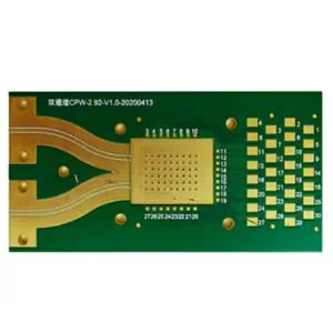
Advanced PCB Manufacturing with Superior Surface Planarity
Our Planar Via PCB technology revolutionizes circuit board design by eliminating traditional via protrusions, creating completely flush surfaces that enhance both performance and reliability. This cutting-edge manufacturing process fills and plates vias to achieve perfect surface planarity, making it ideal for high-density interconnect (HDI) applications and advanced electronic assemblies.
Key Features
Perfect Surface Planarity – Vias are filled and polished flush with the PCB surface, eliminating bumps and depressions that can interfere with component mounting and solder joint integrity.
Enhanced Signal Integrity – Smooth, continuous traces without via-induced impedance discontinuities result in superior high-frequency performance and reduced electromagnetic interference.
Improved Assembly Reliability – Flush surfaces ensure optimal solder paste deposition and component placement accuracy, reducing assembly defects and improving yield rates.
Space Optimization – Enables ultra-compact designs by allowing components to be placed directly over filled vias, maximizing board real estate utilization.
Superior Thermal Management – Filled vias provide excellent thermal conductivity paths while maintaining surface planarity for heat sink mounting and thermal interface materials.
Technical Specifications
- Via sizes: 0.1mm to 0.6mm diameter
- Aspect ratios: Up to 12:1
- Surface roughness: <0.5μm Ra
- Planarity tolerance: ±25μm across entire board
- Compatible with standard PCB materials and finishes
- RoHS compliant and lead-free process compatible
Applications
Perfect for demanding applications including 5G infrastructure, automotive electronics, medical devices, aerospace systems, high-speed computing, and any design requiring maximum component density with uncompromising signal integrity.
Experience the next generation of PCB technology with Planar Via PCBs – where precision meets performance.