Transform Your Electronic Concepts into Production-Ready PCB Designs
Our professional PCB layout design services deliver precision-engineered circuit board layouts that meet the highest industry standards. Whether you’re developing consumer electronics, industrial equipment, or cutting-edge IoT devices, our experienced CAD specialists provide comprehensive PCB design solutions from concept to manufacturing.
What We Offer
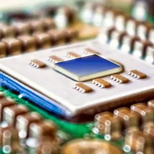
Multi-Layer PCB Design Excellence We specialize in complex multi-layer PCB layouts, from simple 2-layer boards to advanced 16+ layer designs. Our engineers optimize signal integrity, power distribution, and thermal management to ensure your PCB performs flawlessly in real-world applications.
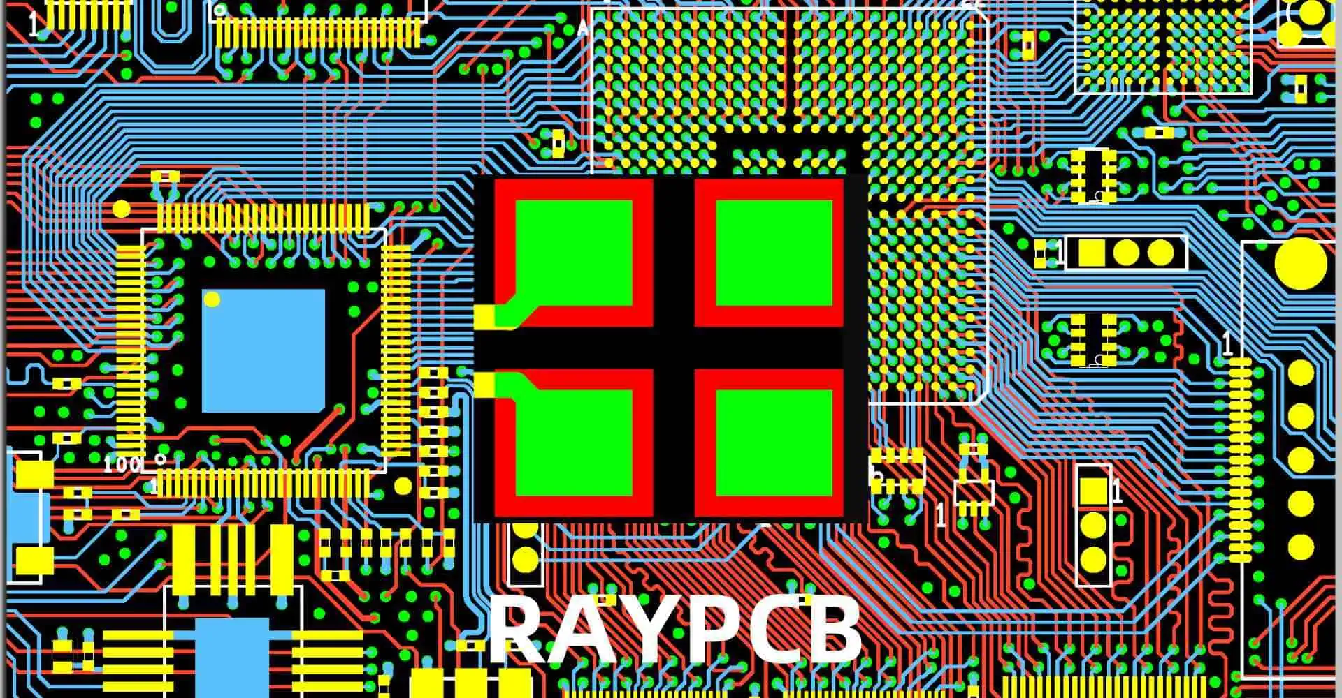
Advanced CAD Software Expertise Our team is proficient in industry-leading PCB design tools including Altium Designer, KiCad, Eagle, and Cadence Allegro. We deliver professional-grade layouts with comprehensive documentation, 3D visualizations, and manufacturing-ready files.
Design Rule Check (DRC) Compliance Every PCB layout undergoes rigorous design rule checking to ensure manufacturability and reliability. We validate electrical rules, spacing requirements, via specifications, and trace routing to eliminate costly manufacturing errors.
Signal Integrity Optimization Critical for high-speed designs, we implement proper impedance control, differential pair routing, and EMI/EMC considerations. Our layouts minimize crosstalk, reduce electromagnetic interference, and maintain signal quality across all operating frequencies.
Key Features
- Schematic to PCB Translation: Seamless conversion from your circuit schematics to optimized PCB layouts
- Component Placement Strategy: Intelligent component positioning for optimal performance and assembly
- Thermal Management: Heat sink placement and thermal via implementation for effective temperature control
- Manufacturing Documentation: Complete fabrication files including Gerber files, drill files, and assembly drawings
- Design for Manufacturing (DFM): Layouts optimized for cost-effective production and high yield rates
Industries We Serve
Our PCB design expertise spans automotive electronics, medical devices, telecommunications, aerospace, consumer products, and industrial automation. We understand the unique requirements and regulatory standards for each sector.
Why Choose Our Services
Proven Track Record: Over20 years of PCB design experience with hundreds of successful projects delivered on time and within budget.
Quality Assurance: Rigorous testing protocols and design verification ensure your PCB meets specifications before manufacturing.
Collaborative Process: We work closely with your engineering team throughout the design process, providing regular updates and incorporating feedback seamlessly.
Fast Turnaround: Efficient project management and streamlined workflows deliver your PCB layouts quickly without compromising quality.
Competitive Pricing: Professional-grade PCB design services at transparent, competitive rates with no hidden fees.
Get Started Today
Ready to bring your electronic design to life? Contact our PCB layout specialists for a free consultation and project quote. We’ll review your requirements, discuss technical specifications, and provide a detailed timeline for your PCB design project.
Professional PCB Layout Design Services – Where Innovation Meets Precision Engineering