The PCB coating process is a crucial step in the manufacturing of printed circuit boards, enhancing their durability, performance, and longevity. This process typically involves several stages, each contributing to the final protective layer on the PCB.
Initially, the PCB undergoes thorough cleaning to remove any contaminants that could interfere with the coating adhesion. This may involve chemical cleaning, plasma treatment, or mechanical abrasion. Once clean, the board is usually pre-heated to ensure optimal coating application.
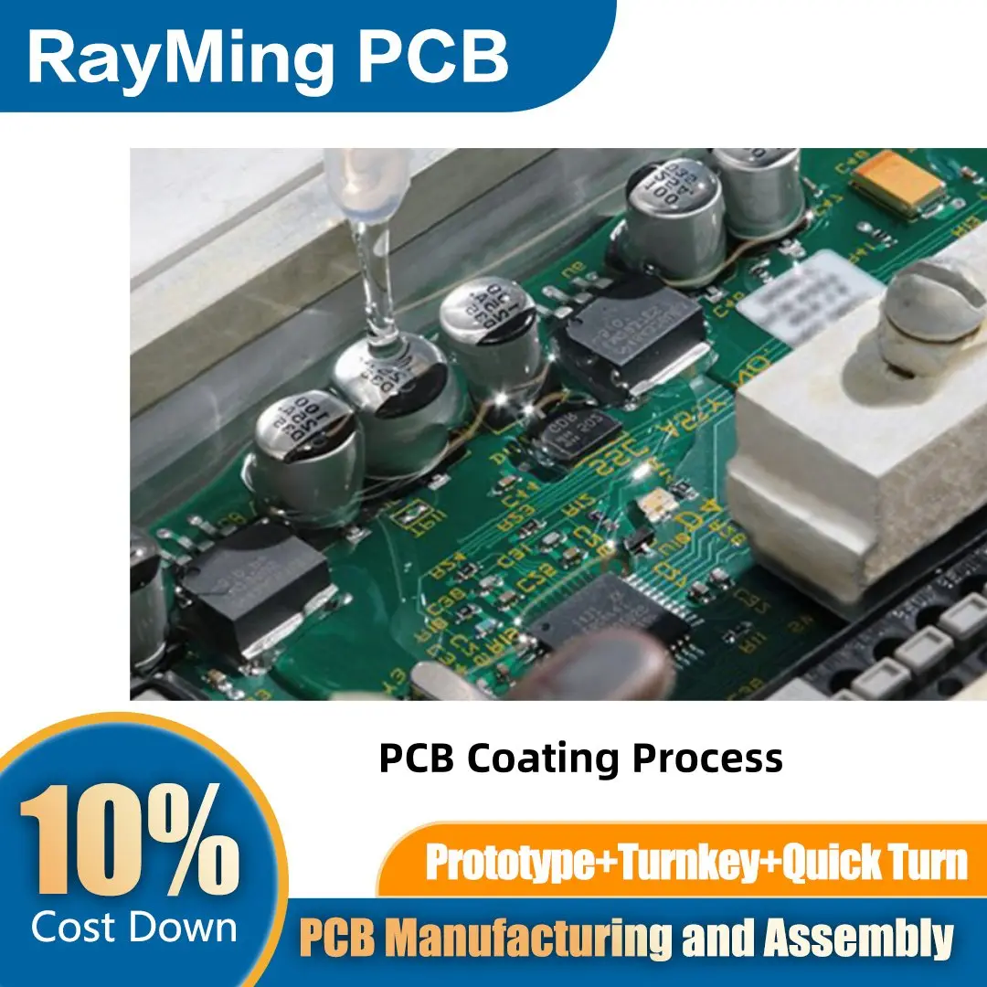
The actual coating application can be done through various methods, depending on the type of coating and desired results. Common techniques include dipping, spraying, brushing, or selective coating using robotic systems. For solder mask application, screen printing or photoimaging processes are often employed.
After application, the coating undergoes a curing process. This can involve heat treatment, UV exposure, or air drying, depending on the coating material. The curing process ensures the coating hardens properly and adheres firmly to the PCB surface.
Quality control checks are performed throughout the process, including thickness measurements and visual inspections, to ensure uniform coverage and identify any defects. Some advanced coating processes may also include additional steps like plasma treatment post-curing to enhance the coating’s properties.
The entire process is carefully controlled to meet specific industry standards and customer requirements, ensuring the PCB is adequately protected for its intended application.