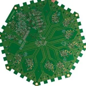
Advanced Microvias for High-Density Interconnect Applications
Our Laser Drilled Via PCBs feature precision-engineered micro vias created using state-of-the-art laser drilling technology. These ultra-small interconnects enable exceptional routing density and signal integrity for today’s most demanding electronic applications.
Key Features
Precision Manufacturing
- Via diameters as small as 25-100 microns with exceptional accuracy
- Aspect ratios up to 1:1 for reliable plating and filling
- Clean, debris-free holes with smooth sidewalls
- Tight positional tolerances (±25 microns typical)
High-Density Capabilities
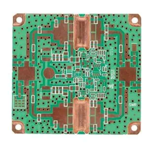
- Support for HDI (High Density Interconnect) designs
- Multiple stacked microvia configurations
- Via-in-pad technology for maximum space utilization
- Compatible with fine-pitch BGA and CSP packages
Superior Performance
- Low inductance and capacitance for high-speed signals
- Excellent signal integrity with minimal crosstalk
- Reliable electrical connections with consistent impedance
- Enhanced thermal management through optimized via placement
Applications
- Mobile Devices: Smartphones, tablets, wearables
- Computing: Processors, memory modules, graphics cards
- Telecommunications: 5G infrastructure, network equipment
- Automotive Electronics: ADAS systems, infotainment
- Medical Devices: Implantables, diagnostic equipment
- Aerospace: Avionics, satellite communications
Technical Specifications
- Via Diameter Range: 25-150 microns
- Drill Depth: Up to 200 microns per layer
- Layer Support: 4-20+ layers
- Substrate Materials: FR-4, polyimide, PTFE, ceramic
- Plating Options: Copper, gold, silver finishes available
- Design Rules: Compatible with IPC-2226 standards
Manufacturing Advantages
Our laser drilling process ensures consistent quality and repeatability while maintaining cost-effectiveness for both prototype and production volumes. The non-contact drilling method eliminates mechanical stress and enables complex via geometries not possible with traditional drilling methods.
Quality Assurance: Each PCB undergoes comprehensive electrical testing and visual inspection to guarantee via integrity and performance reliability.
Contact our engineering team for custom specifications and design consultation to optimize your HDI PCB requirements.