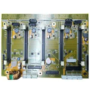
Hematology analyzers are sophisticated medical devices used to perform blood cell counts and analyses. The printed circuit board (PCB) is a crucial component in these analyzers, serving as the foundation for the electronic systems that control the device’s operations. This article delves into the intricacies of designing and manufacturing PCBs for hematology analyzers.
PCB Design Considerations
1. High-Speed Signal Integrity
Hematology analyzers process large amounts of data quickly, requiring high-speed circuits. The PCB design must account for signal integrity to ensure accurate and reliable results. This involves:
- Controlled impedance routing
- Proper stackup design to minimize crosstalk
- Use of ground planes and power planes for noise reduction
- Careful placement of decoupling capacitors
2. Analog and Digital Separation
Hematology analyzers often combine analog and digital circuits. Keeping these separate is crucial to prevent noise interference:
- Use of split ground planes
- Strategic component placement to isolate sensitive analog circuits
- Proper use of guard traces and shielding techniques
3. Thermal Management
The analyzer’s continuous operation can generate significant heat. PCB design must incorporate thermal management strategies:
- Use of thermal vias under heat-generating components
- Copper pours for heat dissipation
- Strategic placement of components to optimize airflow
4. EMI/EMC Considerations
To comply with medical device regulations, the PCB must be designed with electromagnetic interference (EMI) and electromagnetic compatibility (EMC) in mind:
- Proper grounding and shielding techniques
- Use of ferrite beads and common-mode chokes
- EMI suppression components placement
5. Component Selection
Choosing the right components is crucial for the analyzer’s performance and reliability:
- High-precision analog components for accurate measurements
- Robust digital components capable of high-speed data processing
- Components rated for medical use and with appropriate certifications
Manufacturing Process
1. Material Selection
The choice of PCB material is critical:
- FR-4 is commonly used, but high-frequency applications may require specialized materials like Rogers or Taconic
- Consider the dielectric constant and loss tangent of materials for high-frequency circuits
2. Layer Stackup
Hematology analyzer PCBs often require multilayer designs:
- 6 to 12 layers are common, depending on complexity
- Proper stackup design is crucial for impedance control and EMI suppression
3. Fabrication Techniques
Advanced fabrication techniques may be necessary:
- Fine line and space for high-density designs
- Blind and buried vias for complex routing
- Controlled depth drilling for impedance matching
4. Surface Finish
The surface finish affects solderability and long-term reliability:
- ENIG (Electroless Nickel Immersion Gold) is often preferred for its excellent solderability and protection against oxidation
- Other options include HASL (Hot Air Solder Leveling) or OSP (Organic Solderability Preservative)
5. Assembly Considerations
The assembly process must adhere to stringent quality standards:
- Use of lead-free solder in compliance with RoHS regulations
- Automated optical inspection (AOI) and X-ray inspection for quality control
- Implementation of IPC class 3 standards for medical devices
6. Testing and Validation
Rigorous testing is essential:
- In-circuit testing (ICT) for manufacturing defects
- Functional testing to ensure proper operation
- Environmental stress screening to simulate real-world conditions
Regulatory Compliance
Hematology analyzer PCBs must comply with various regulations:
- FDA requirements for medical devices
- IEC 60601-1 for medical electrical equipment safety
- ISO 13485 for quality management systems in medical devices