Transform Your Circuit Designs into Reality with Professional-Grade Prototypes
Our Functional PCB Prototypes deliver fully operational engineering samples that bridge the gap between your design concepts and production-ready circuits. These aren’t just visual mockups – they’re complete, testable prototypes engineered to validate your designs, verify functionality, and accelerate your development timeline.
Key Features
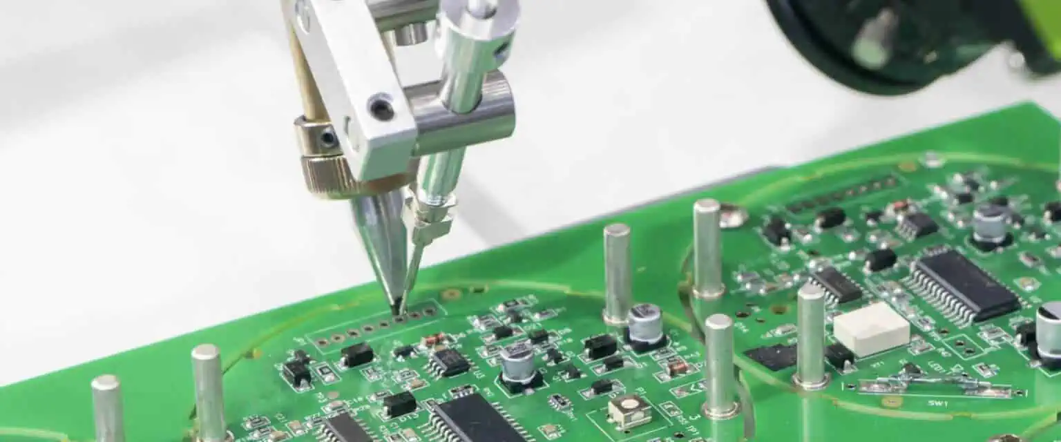
Fully Functional Testing – Every prototype arrives ready for immediate electrical testing and validation. Components are professionally assembled and circuits are verified to ensure your design performs exactly as intended.
Rapid Turnaround – From design files to working prototypes in as little as 5-7 business days. Our streamlined manufacturing process eliminates lengthy delays that slow down your development cycle.
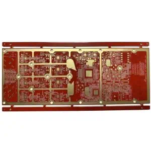
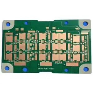
Engineering-Grade Quality – Built using the same materials and processes as production PCBs, including FR4 substrates, professional surface finishes, and precise component placement for reliable performance.
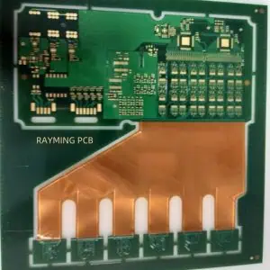
Multi-Layer Capabilities – Support for complex designs from simple 2-layer boards to advanced 12+ layer configurations with controlled impedance, blind/buried vias, and HDI technology.
Component Flexibility – Compatible with a wide range of components including SMD, through-hole, BGA, QFN, and specialty parts. We source components or work with your supplied bill of materials.
Applications
Perfect for product development teams, electronics engineers, startups, and research institutions validating new designs, testing circuit functionality, demonstrating proof-of-concept prototypes, or preparing for pilot production runs.
What’s Included: Assembled PCB prototype(s), basic electrical testing report, component placement verification, and technical support for any assembly questions.
Ready to bring your circuit designs to life? Upload your Gerber files and BOM today to receive a detailed quote and timeline for your functional PCB prototypes.