Ultra-Compact Semiconductor Packaging Solution
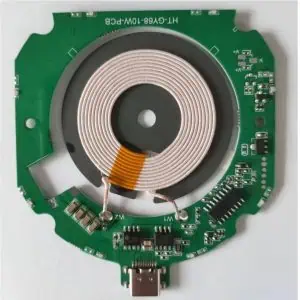
The CSP PCB (Chip Scale Package Substrate) represents cutting-edge miniaturization technology designed for space-critical electronic applications. This advanced substrate solution enables direct chip mounting with package dimensions nearly identical to the actual semiconductor die size, maximizing board real estate efficiency.
Key Features:
- Minimal Footprint: Package size within 1.2x of the original die dimensions
- High-Density Interconnect: Fine-pitch ball grid array (BGA) or land grid array (LGA) configurations
- Superior Electrical Performance: Reduced parasitic inductance and capacitance for enhanced signal integrity
- Thermal Efficiency: Optimized heat dissipation pathways for improved thermal management
- Multi-Layer Construction: Advanced laminate technology supporting complex routing requirements
Technical Specifications:
- Substrate thickness: 0.1mm – 0.3mm
- Ball pitch: 0.4mm – 0.8mm
- Layer count: 2-8 layers
- Via diameter: 50-100 microns
- Operating temperature: -40°C to +125°C
- Dielectric materials: FR-4, polyimide, or advanced low-loss substrates
Applications:
- Mobile devices and smartphones
- Wearable electronics
- IoT sensors and modules
- Memory modules (DDR, NAND Flash)
- Microprocessors and microcontrollers
- RF and wireless communication chips
Advantages:
- Reduced PCB area requirements by up to 60%
- Lower assembly costs through simplified manufacturing
- Enhanced electrical performance and signal speed
- Improved reliability through shorter interconnect paths
- Enables ultra-thin device designs
Ideal for next-generation electronics where size, weight, and performance are critical design parameters. Compatible with standard SMT assembly processes and available in custom configurations to meet specific application requirements.